Photonics Research, 2019, 7 (10): 10001127, Published Online: Sep. 9, 2019  

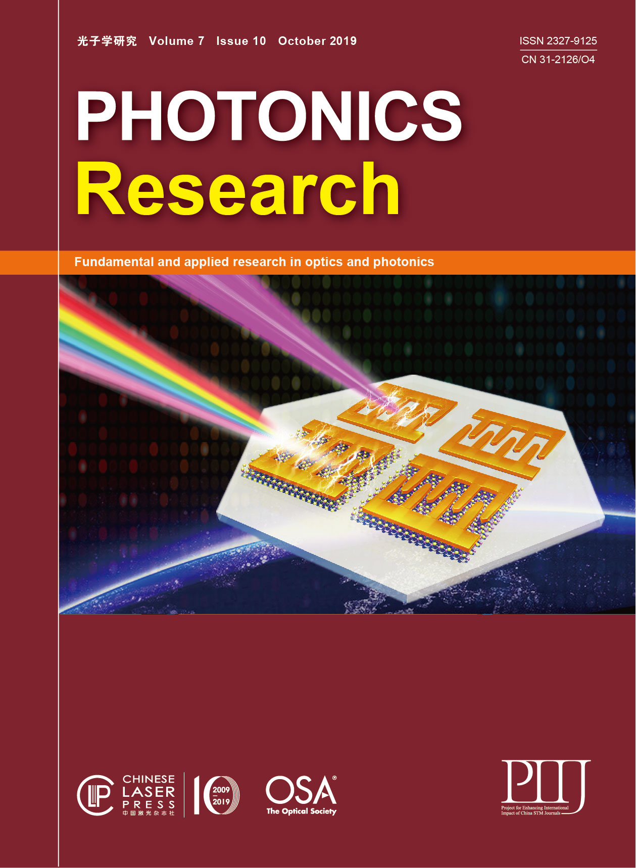
Monolithic integration of MoS2-based visible detectors and GaN-based UV detectors Download: 738次

Author Affiliations
1 State Key Laboratory of Luminescence and Applications, Changchun Institute of Optics, Fine Mechanics and Physics, Chinese Academy of Sciences, Changchun 130033, China
2 Center of Materials Science and Optoelectronics Engineering, University of Chinese Academy of Sciences, Beijing 100049, China
3 Department of Electrical and Computer Engineering, National University of Singapore, Singapore 117583, Singapore
4 Shenzhen Castle Security Technology Co., Ltd., Shenzhen 518000, China
5 State Key Laboratory of Functional Materials for Informatics, Shanghai Institute of Microsystem and Information Technology, Chinese Academy of Sciences, Shanghai 200050, China
6 e-mail: liuxinke@ciomp.ac.cn
7 e-mail: lidb@ciomp.ac.cn
Copy Citation Text

You Wu, Zhiwen Li, Kah-Wee Ang, Yuping Jia, Zhiming Shi, Zhi Huang, Wenjie Yu, Xiaojuan Sun, Xinke Liu, Dabing Li. Monolithic integration of MoS2-based visible detectors and GaN-based UV detectors[J]. Photonics Research, 2019, 7(10): 10001127.

References

[1] R. Cao, H. Wang, Z. Guo, D. K. Sang, L. Zhang, Q. Xiao, Y. Zhang, D. Fan, J. Li, H. Zhang. Black phosphorous/indium selenide photoconductive detector for visible and near-infrared light with high sensitivity. Adv. Opt. Mater., 2019, 7: 1900020.

[2] M. Zhao, Z. Ye, R. Suzuki, Y. Ye, H. Zhu, J. Xiao, Y. Wang, Y. Iwasa, X. Zhang. Atomically phase-matched second-harmonic generation in a 2D crystal. Light Sci. Appl., 2016, 5: e16131.

[3] A. K. Geim, I. V. Grigorieva. Van der Waals heterostructures. Nature, 2013, 499: 419-425.

[4] Z. Guo, S. Chen, Z. Wang, Z. Yang, F. Liu, Y. Xu, J. Wang, Y. Yi, H. Zhang, L. Liao, P. K. Chu, X.-F. Yu. Metal-ion-modified black phosphorus with enhanced stability and transistor performance. Adv. Mater., 2017, 29: 1703811.

[5] K. S. Novoselov, A. Mishchenko, A. Carvalho, A. H. C. Neto. 2D materials and van der Waals heterostructures. Science, 2016, 353: aac9439.

[6] Y. Abate, S. Gamage, Z. Li, V. Babicheva, M. H. Javani, H. Wang, S. B. Cronin, M. I. Stockman. Nanoscopy reveals surface-metallic black phosphorus. Light Sci. Appl., 2016, 5: e16162.

[7] M. Zhang, Q. Wu, F. Zhang, L. Chen, X. Jin, Y. Hu, Z. Zheng, H. Zhang. 2D black phosphorus saturable absorbers for ultrafast photonics. Adv. Opt. Mater., 2019, 7: 1800224.

[8] J. Yang, R. Xu, J. Pei, Y. W. Myint, F. Wang, Z. Wang, S. Zhang, Z. Yu, Y. Lu. Optical tuning of exciton and trion emissions in monolayer phosphorene. Light Sci. Appl., 2015, 4: e312.

[9] Q. Ou, Y. Zhang, Z. Wang, J. A. Yuwono, R. Wang, Z. Dai, W. Li, C. Zheng, Z.-Q. Xu, X. Qi, S. Duhm, N. V. Medhekar, H. Zhang, Q. Bao. Strong depletion in hybrid perovskite p-n junctions induced by local electronic doping. Adv. Mater., 2018, 30: 1705792.

[10] Y. Zhang, C.-K. Lim, Z. Dai, G. Yu, J. W. Haus, H. Zhang, P. N. Prasad. Photonics and optoelectronics using nano-structured hybrid perovskite media and their optical cavities. Phys. Rep., 2019, 795: 1-51.

[11] J. Wang, I. Verzhbitskiy, G. Eda. Electroluminescent devices based on 2D semiconducting transition metal dichalcogenides. Adv. Mater., 2018, 30: 1802687.

[12] K. F. Mak, J. Shan. Photonics and optoelectronics of 2D semiconductor transition metal dichalcogenides. Nat. Photonics, 2016, 10: 216-226.

[13] J. Y. Lee, J.-H. Shin, G.-H. Lee, C.-H. Lee. Two-dimensional semiconductor optoelectronics based on van der Waals heterostructures. Nanomaterials, 2016, 6: 193.

[14] M. Buscema, J. O. Island, D. J. Groenendijk, S. I. Blanter, G. A. Steele, H. S. J. van der Zant, A. Castellanos-Gomez. Photocurrent generation with two-dimensional van der Waals semiconductors. Chem. Soc. Rev., 2015, 44: 3691-3718.

[15] S. Manzeli, D. Ovchinnikov, D. Pasquier, O. V. Yazyev, A. Kis. 2D transition metal dichalcogenides. Nat. Rev. Mater., 2017, 2: 17033.

[16] Z. Yin, H. Li, H. Li, L. Jiang, Y. Shi, Y. Sun, G. Lu, Q. Zhang, X. Chen, H. Zhang. Single-layer MoS2 phototransistors. ACS Nano, 2012, 6: 74-80.

[17] N. Liu, P. Kim, J. H. Kim, J. H. Ye, S. Kim, C. J. Lee. Large-area atomically thin MoS2 nanosheets prepared using electrochemical exfoliation. ACS Nano, 2014, 8: 6902-6910.

[18] Y. Yang, H. Hou, G. Zou, W. Shi, H. Shuai, J. Li, X. Ji. Electrochemical exfoliation of graphene-like two-dimensional nanomaterials. Nanoscale, 2019, 11: 16-33.

[19] R. Zhuo, Y. Wang, D. Wu, Z. Lou, Z. Shi, T. Xu, J. Xu, Y. Tian, X. Li. High-performance self-powered deep ultraviolet photodetector based on MoS2/GaN p-n heterojunction. J. Mater. Chem. C, 2018, 6: 299-303.

[20] N. Goel, R. Kumar, B. Roul, M. Kumar, S. B. Krupanidhi. Wafer-scale synthesis of a uniform film of few-layer MoS2 on GaN for 2D heterojunction ultraviolet photodetector. J. Phys. D, 2018, 51: 374003.

[21] W. Zhang, J.-K. Huang, C.-H. Chen, Y.-H. Chang, Y.-J. Cheng, L.-J. Li. High-gain phototransistors based on a CVD MoS2 monolayer. Adv. Mater., 2013, 25: 3456-3461.

[22] X. Ling, Y. Lee, Y. Lin, W. Fang, L. Yu, M. S. Dresselhaus, J. Kong. Role of the seeding promoter in MoS2 growth by chemical vapor deposition. Nano Lett., 2014, 14: 464-472.

[23] H. Shan, Y. Yu, X. Wang, Y. Luo, S. Zu, B. Du, T. Han, B. Li, Y. Li, J. Wu, F. Lin, K. Shi, B. Tay, Z. Liu, X. Zhu, Z. Fang. Direct observation of ultrafast plasmonic hot electron transfer in the strong coupling regime. Light Sci. Appl., 2019, 8: 9.

[24] O. Lopez-Sanchez, D. Lembke, M. Kayci, A. Radenovic, A. Kis. Ultrasensitive photodetectors based on monolayer MoS2. Nat. Nanotechnol., 2013, 8: 497-501.

[25] N. Perea-López, Z. Lin, N. R. Pradhan, A. Iñiguez-Rábago, A. L. Elías, A. McCreary, J. Lou, P. M. Ajayan, H. Terrones, L. Bali, M. Terrones. CVD-grown monolayered MoS2 as an effective photosensor operating at low-voltage. 2D Mater., 2014, 1: 011004.

[26] Z. Cheng, M. Xia, S. Liu, R. Hu, G. Liang, S. Zhang. Role of rough substrate on the growth of large single-crystal MoS2 by chemical vapor deposition. Appl. Surf. Sci., 2019, 476: 1008-1015.

[27] D. Dumcenco, D. Ovchinnikov, K. Marinov, P. Lazi, M. Gibertini, N. Marzari, O. L. Sanchez, Y.-C. Kung, D. Krasnozhon, M.-W. Chen, S. Bertolazzi, P. Gillet, A. F. I. Morral, A. Radenovic, A. Kis. Large-area epitaxial monolayer MoS2. ACS Nano, 2015, 9: 4611-4620.

[28] X. Liu, Y. Chen, D. Li, S.-W. Wang, C.-C. Ting, L. Chen, K.-W. Ang, C.-W. Qiu, Y.-L. Chuen, X. Sun, H.-C. Kuo. Nearly lattice-matched molybdenum disulfide/gallium nitride heterostructure enabling high-performance phototransistors. Photon. Res., 2019, 7: 311-317.

[29] P. Yan, J. Wang, G. Yang, N. Lu, G. Chu, X. Zhang, X. Shen. Chemical vapor deposition of monolayer MoS2 on sapphire, Si and GaN substrates. Superlattices Microstruct., 2018, 120: 235-240.

[30] Y. Wan, J. Xiao, J. Li, X. Fang, K. Zhang, L. Fu, P. Li, Z. Song, H. Zhang, Y. Wang, M. Zhao, J. Lu, N. Tang, G. Ran, X. Zhang, Y. Ye, L. Dai. Epitaxial single-layer MoS2 on GaN with enhanced valley helicity. Adv. Mater., 2018, 30: 1703888.

[31] R. Murray, B. L. Evans. The thermal expansion of 2H-MoS2 and 2H-WSe2 between 10 and 320 K. J. Appl. Crystallogr., 1979, 12: 312-315.

[32] K. Wang, R. R. Reeber. Thermal expansion of GaN and AlN. Mat. Res. Soc. Symp. Proc., 1998, 12: 863-868.

[33] D. Li, K. Jiang, X. Sun, C. Guo. AlGaN photonics: recent advances in materials and ultraviolet devices. Adv. Opt. Photon., 2018, 10: 43-110.

[34] C.-Y. Huang, C. Chang, G.-Z. Lu, W.-C. Huang, C.-S. Huang, M.-L. Chen, T.-N. Lin, J.-L. Shen, T.-Y. Lin. Hybrid 2D/3D MoS2/GaN heterostructures for dual functional photoresponse. Appl. Phys. Lett., 2018, 112: 233106.

[35] X. Liu, J. He, Q. Liu, D. Tang, J. Wen, W. Liu, W. Yu, J. Wu, Z. He, Y. Lu, D. Zhu, W. Liu, P. Cao, S. Han, K.-W. Ang. Low temperature carrier transport study of monolayer MoS2 field effect transistors prepared by chemical vapor deposition under an atmospheric pressure. J. Appl. Phys., 2015, 118: 124506.

[36] K.-G. Zhou, F. Withers, Y. Cao, S. Hu, G. Yu, C. Casiraghi. Raman modes of MoS2 used as fingerprint of vander Waals interactions in 2-D crystal-based heterostructures. ACS Nano, 2014, 8: 9914-9924.

[37] C. Lee, H. G. Yan, L. E. Brus, T. F. Heinz, J. Hone, S. Ryu. Anomalous lattice vibrations of single-and few-layer MoS2. ACS Nano, 2010, 4: 2695-2700.

[38] P. Yan, Q. Tian, G. Yang, Y. Weng, Y. Zhang, J. Wang, F. Xie, N. Lu. Epitaxial growth and interfacial property of monolayer MoS2 on gallium nitride. RSC Adv., 2018, 8: 33193-33197.

[39] H. Siegle, G. Kaczmarczyk, L. Filippidis, A. P. Litvinchuk, A. Hoffmann, C. Thomsen. Zone-boundary phonons in hexagonal and cubic GaN. Phys. Rev. B, 1997, 55: 7000-7004.

[40] V. Y. Davydov, Y. E. Kitaev, I. N. Goncharuk, A. N. Smirnov. Phonon dispersion and Raman scattering in hexagonal GaN and AlN. Phys. Rev. B, 1998, 58: 12899.

[41] K. F. Mak, C. Lee, J. Hone, J. Shan, T. F. Heinz. Atomically thin MoS2: a new direct-gap semiconductor. Phys. Rev. Lett., 2010, 105: 136805.

[42] A. Splendiani, L. Sun, Y. Zhang, T. Li, J. Kim, C.-Y. Chim, G. L. Galli, F. Wang. Emerging photoluminescence in monolayer MoS2. Nano Lett., 2010, 10: 1271-1275.

[43] W. Choi, M. Y. Cho, A. Konar, J. H. Lee, G. Cha, S. C. Hong, S. Kim, J. Kim, D. Jena, J. Joo, S. Kim. High-detectivity multilayer MoS2 phototransistors with spectral response from ultraviolet to infrared. Adv. Mater., 2012, 24: 5832-5836.

[44] L. Liu, C. Yang, A. Patanè, Z. Yu, F. Yan, K. Wang, H. Lu, J. Li, L. Zhao. High-detectivity ultraviolet photodetectors based on laterally mesoporous GaN. Nanoscale, 2017, 9: 8142-8148.

[45] D. Li, X. Sun, H. Song, Z. Li, Y. Chen, H. Jiang, G. Miao. Realization of a high-performance GaN UV detector by nanoplasmonic enhancement. Adv. Mater., 2012, 24: 845-849.

[46] S. Li, X. Chen, F. Liu, Y. Chen, B. Liu, W. Deng, B. An, F. Chu, G. Zhang, S. Li, X. Li, Y. Zhang. Enhanced performance of a CVD MoS2 photodetector by chemical in situ n-type doping. ACS Appl. Mater. Interfaces, 2019, 11: 11636-11644.

[47] F. Gong, F. Wu, M. Long, F. Chen, M. Su, Z. Yang, J. Shi. Black phosphorus infrared photodetectors with fast response and high photoresponsivity. Phys. Status Solidi (RRL), 2018, 12: 1800310.

[48] J.-Y. Wu, Y. T. Chun, S. Li, T. Zhang, J. Wang, P. K. Shrestha, D. Chu. Broadband MoS2 field-effect phototransistors: ultrasensitive visible-light photoresponse and negative infrared photoresponse. Adv. Mater., 2018, 30: 1705880.

[49] P. Hu, L. Wang, M. Yoon, J. Zhang, W. Feng, X. Wang, Z. Wen, J. C. Idrobo, Y. Miyamoto, D. B. Geohegan, K. Xiao. Highly responsive ultrathin GaS nanosheet photodetectors on rigid and flexible substrates. Nano Lett., 2013, 13: 1649-1654.

[50] Y. Guo, G. Yu, Y. Liu. Functional organic field-effect transistors. Adv. Mater., 2010, 22: 4427-4447.

[51] X. Gong, M. Tong, Y. Xia, W. Cai, J. S. Moon, Y. Cao, G. Yu, C.-L. Shieh, B. Nilsson, A. J. Heeger. High-detectivity polymer photodetectors with spectral response from 300 nm to 1450 nm. Science, 2009, 325: 1665-1667.

[52] F. Xia, T. Mueller, Y.-M. Lin, A. Valdes-Garcia, P. Avouris. Ultrafast graphene photodetector. Nat. Nanotechnol., 2009, 4: 839-843.

You Wu, Zhiwen Li, Kah-Wee Ang, Yuping Jia, Zhiming Shi, Zhi Huang, Wenjie Yu, Xiaojuan Sun, Xinke Liu, Dabing Li. Monolithic integration of MoS2-based visible detectors and GaN-based UV detectors[J]. Photonics Research, 2019, 7(10): 10001127.

引用该论文: TXT   |   EndNote

相关论文

加载中...

关于本站 Cookie 的使用提示

中国光学期刊网使用基于 cookie 的技术来更好地为您提供各项服务,点击此处了解我们的隐私策略。 如您需继续使用本网站,请您授权我们使用本地 cookie 来保存部分信息。
全站搜索
您最值得信赖的光电行业旗舰网络服务平台!