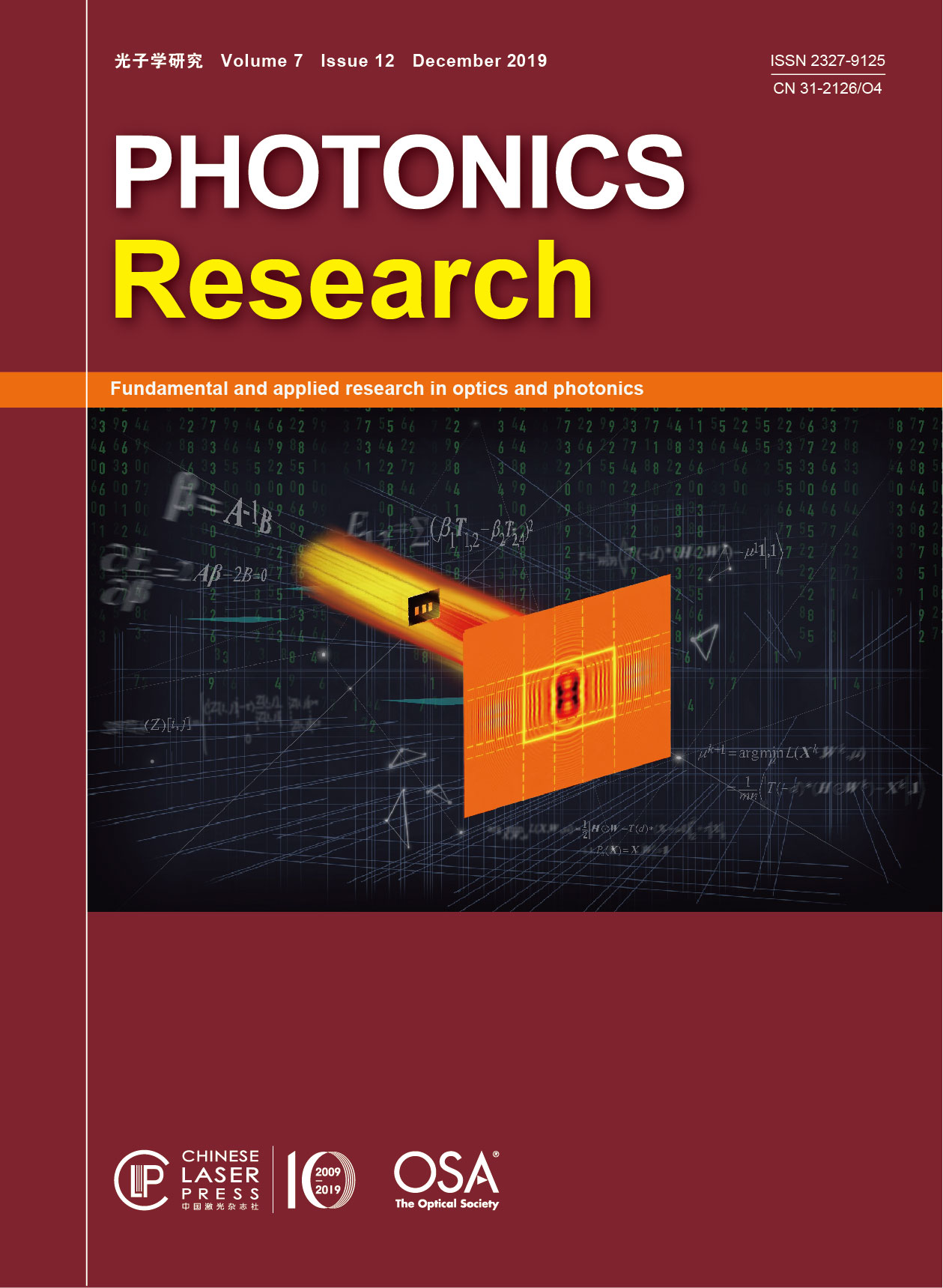
Photonics Research, 2019, 7 (12): 12001511, Published Online: Nov. 28, 2019  

Absorption and emission modulation in a MoS2–GaN (0001) heterostructure by interface phonon–exciton coupling Download: 735次

Author Affiliations
1 Department of Physics, University of North Texas, Denton, Texas 76203, USA
2 Department of Chemistry, University of North Texas, Denton, Texas 76203, USA
3 Department of Physics, Northeastern University, Boston, Massachusetts 02115, USA
Abstract
Semiconductor heterostructures based on layered two-dimensional transition metal dichalcogenides (TMDs) interfaced to gallium nitride (GaN) are excellent material systems to realize broadband light absorbers and emitters due to their close proximity in the lattice constants. The surface properties of a polar semiconductor such as GaN are dominated by interface phonons, and thus the optical properties of the vertical heterostructure are influenced by the coupling of these carriers with phonons. The activation of different Raman modes in the heterostructure caused by the coupling between interfacial phonons and optically generated carriers in a monolayer MoS2–GaN (0001) heterostructure is observed. Different excitonic states in MoS2 are close to the interband energy state of intraband defect state of GaN. Density functional theory (DFT) calculations are performed to determine the band alignment of the interface and revealed a type-I heterostructure. The close proximity of the energy levels and the excitonic states in the semiconductors and the coupling of the electronic states with phonons result in the modification of carrier relaxation rates. Modulation of the excitonic absorption states in MoS2 is measured by transient optical pump-probe spectroscopy and the change in emission properties of both semiconductors is measured by steady-state photoluminescence (PL) emission spectroscopy. There is significant red-shift of the C excitonic band and faster dephasing of carriers in MoS2. However, optical excitation at energy higher than the bandgap of both semiconductors slows down the dephasing of carriers and energy exchange at the interface. Enhanced and blue-shifted PL emission is observed in MoS2. GaN band-edge emission is reduced in intensity at room temperature due to increased phonon-induced scattering of carriers in the GaN layer. Our results demonstrate the relevance of interface coupling between the semiconductors for the development of optical and electronic applications.

Yuba Poudel, Jagoda Sławińska, Priya Gopal, Sairaman Seetharaman, Zachariah Hennighausen, Swastik Kar, Francis D’souza, Marco Buongiorno Nardelli, Arup Neogi. Absorption and emission modulation in a MoS2–GaN (0001) heterostructure by interface phonon–exciton coupling[J]. Photonics Research, 2019, 7(12): 12001511.

引用该论文: TXT   |   EndNote

相关论文

加载中...

关于本站 Cookie 的使用提示

中国光学期刊网使用基于 cookie 的技术来更好地为您提供各项服务,点击此处了解我们的隐私策略。 如您需继续使用本网站,请您授权我们使用本地 cookie 来保存部分信息。
全站搜索
您最值得信赖的光电行业旗舰网络服务平台!