Photonics Research, 2019, 7 (8): 08000828, Published Online: Jul. 11, 2019
Ge-on-Si modulators operating at mid-infrared wavelengths up to 8 μm
Figures & Tables
Fig. 1. (a) Schematic of the PIN junction modulator cross section. (b) The mode profiles for Ge-on-Si rib waveguides at 3.8 and 8 μm wavelengths, modeled using Lumerical Mode Solutions.
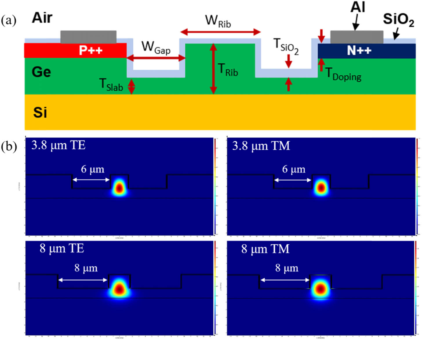
Fig. 2. Schematic illustration of the process flow used for the fabrication of Ge-on-Si waveguide modulators.

Fig. 3. Optical microscope images of the EAM devices at 3.8 μm. The image is composed of two images that have been stitched together, since the 1-mm PIN diode length does not fit in the microscope field of view. The horizontal white strip near the middle of the figure separates the two parts.

Fig. 4. Top view scanning electron microscope image of the PIN diode. The waveguide and etched lateral cladding are in the middle of the image in grey. The blue shaded region on the left is N++ doped, while the red region on the right is P++ doped. On both the P++- and N++-doped side regions, rough surfaces are visible, the areas in which vias through the SiO 2

Fig. 5. Schematic diagram of the experimental setup for modulator characterization (PPG, pulse pattern generator).

Fig. 6. (a) Modulation depth as a function of the wavelength under different bias conditions. (b) Modulation depth as a function of current at a wavelength of 3765 nm. Inset: current-voltage device characteristic.

Fig. 7. (a) Optical spectra of the MZM under several DC voltages. The spectral transmission is normalized to the highest transmission as seen through the device (so that the offset of transmission from zero does not represent the insertion loss). (b) Phase shift versus current of the MZM.


Fig. 9. Captured LWIR camera image with the QCL tuned to λ = 8 μm

Fig. 10. (a) Extinction ratio as a function of the applied voltage for a 2-mm-long EAM operating at a wavelength of 8 μm. Inset: current per unit length versus voltage curves at a wavelength of 8 μm (2-mm-long diode) and of 3.8 μm (1-mm-long diode) for EAM devices with the same 8-μm contact separation (W Gap W Gap

Tiantian Li, Milos Nedeljkovic, Nannicha Hattasan, Wei Cao, Zhibo Qu, Callum G. Littlejohns, Jordi Soler Penades, Lorenzo Mastronardi, Vinita Mittal, Daniel Benedikovic, David J. Thomson, Frederic Y. Gardes, Hequan Wu, Zhiping Zhou, Goran Z. Mashanovich. Ge-on-Si modulators operating at mid-infrared wavelengths up to 8 μm[J]. Photonics Research, 2019, 7(8): 08000828.


 PDF全文
PDF全文

