Chinese Optics Letters, 2018, 16 (7): 070901, Published Online: Jul. 19, 2018  

Mode division multiplexed holography by out-of-plane scattering of plasmon/guided modes Download: 575次

Author Affiliations
National Laboratory of Solid State Microstructures, College of Engineering and Applied Sciences, Collaborative Innovation Center of Advanced Microstructures, Nanjing University, Nanjing 210093, China
Figures & Tables

Fig. 1. (a) Calculated mode effective index of the DLPW with respect to different SiO2 layer thickness including all TE and TM modes. (b) The normalized loss measurement of SPP, TE, and TM modes. The symbols are the experimental data and the curves are the exponential fittings. The orange horizontal dotted line means the guided wave’s intensity attenuated to 1/e.

下载图片 查看原文

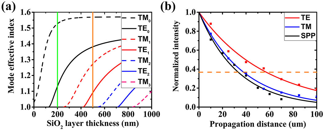
Fig. 2. (a) Illustration of the experimental setup; (b) a schematic of the DLPW where multiple modes are launched by a grating in the silver film from an incident laser beam and image over our sample; (c) a top-view scanning electron microscope (SEM) image of the couple-in grating and nanoscatterers in which the inset figure is the zoom-in image showing the details of the hologram units.

下载图片 查看原文

Fig. 3. Schematic of the guided-mode propagating through a well-designed hologram for (a) TM0 and (c) TE0 along the +x direction; (b) and (d) are the calculation results by the diffraction Huygens–Fresnel principle with respect to the hologram structures under TM0 and TE0 illumination, respectively. The size is 30μm×30μm.

下载图片 查看原文

Fig. 4. (a) and (b) The 30μm×30μm hologram patterns of a single object letter ‘E’ with respect to the TE0 mode as the reference wave and letter ‘M’ with respect to the TM0 mode as the reference wave, respectively; (c) the overlapped hologram pattern for two holographic images, and (d) the zoom-in figure; (e) shared scatterers between two hologram patterns; (f) the final designed hologram structure with a well-selected nanoscatterers array.

下载图片 查看原文

Fig. 5. (a) and (c) The SEM images of a couple-in grating and a multiplexed hologram by TE0 and TM0. The size of the nanoscatterers array is 30μm×30μm due to the loss of TM mode. The red arrow in the upper-right corner represents the polarization of the incident lights and the red arrow in the center-left with the letters ‘TE’ or ‘TM’ represents the excited guided mode. (b) and (d) The experimental measurements of the capital letters ‘E’ and ‘M’ images decoded from the multiplexed hologram according to TE and TM mode excitation, respectively.

下载图片 查看原文

Fig. 6. (a) and (c) The SEM images of the totally same multiplexed hologram by TE0 and TE1 but different couple-in gratings with different periods. The size of the nanoscatterers arrays is 60μm×60μm due to the low loss of the TE mode. The periods of the gratings in (a) and (c) are equal to the effective wavelengths of TE0 and TE1, respectively. (b) and (d) The experimental measurements of the number ‘0’ and ‘1’ images decoded from the multiplexed hologram according to TE0 and TE1 mode excitation, respectively.

下载图片 查看原文

Chenchen Zhao, Ji Chen, Hanmeng Li, Tao Li, Shining Zhu. Mode division multiplexed holography by out-of-plane scattering of plasmon/guided modes[J]. Chinese Optics Letters, 2018, 16(7): 070901.

引用该论文: TXT   |   EndNote

相关论文

加载中...

关于本站 Cookie 的使用提示

中国光学期刊网使用基于 cookie 的技术来更好地为您提供各项服务,点击此处了解我们的隐私策略。 如您需继续使用本网站,请您授权我们使用本地 cookie 来保存部分信息。
全站搜索
您最值得信赖的光电行业旗舰网络服务平台!