Chinese Optics Letters, 2020, 18 (9): 092401, Published Online: Jul. 15, 2020   

Plasmonic Luneburg lens and plasmonic nano-coupler Download: 691次

Lei Zhang 1,2Lin Wang 1,2Yanqing Wu 1,3,*Renzhong Tai 1,3,**
Author Affiliations
1 Shanghai Institute of Applied Physics, Chinese Academy of Sciences, Shanghai 201800, China
2 University of Chinese Academy of Sciences, Beijing 100049, China
3 Shanghai Synchrotron Radiation Facility, Shanghai Advanced Research Institute, Chinese Academy of Sciences, Shanghai 201204, China
Figures & Tables

Fig. 1. (a) Schematic diagram for a PMLL. (b) Quarter enlarged view of the top of the dielectric film with air holes. (c) Transverse cross section of the intensity profile at the point ρ=R in the y direction. (d) Intensity distribution of SPPs [three-dimensional (3D) simulation] propagating along y direction and passing through a PMLL. The red circle indicates the radius R of the PMLL. The red dotted circle indicates the real area of the designed lens. The white dotted line indicates the position y=R.

下载图片 查看原文

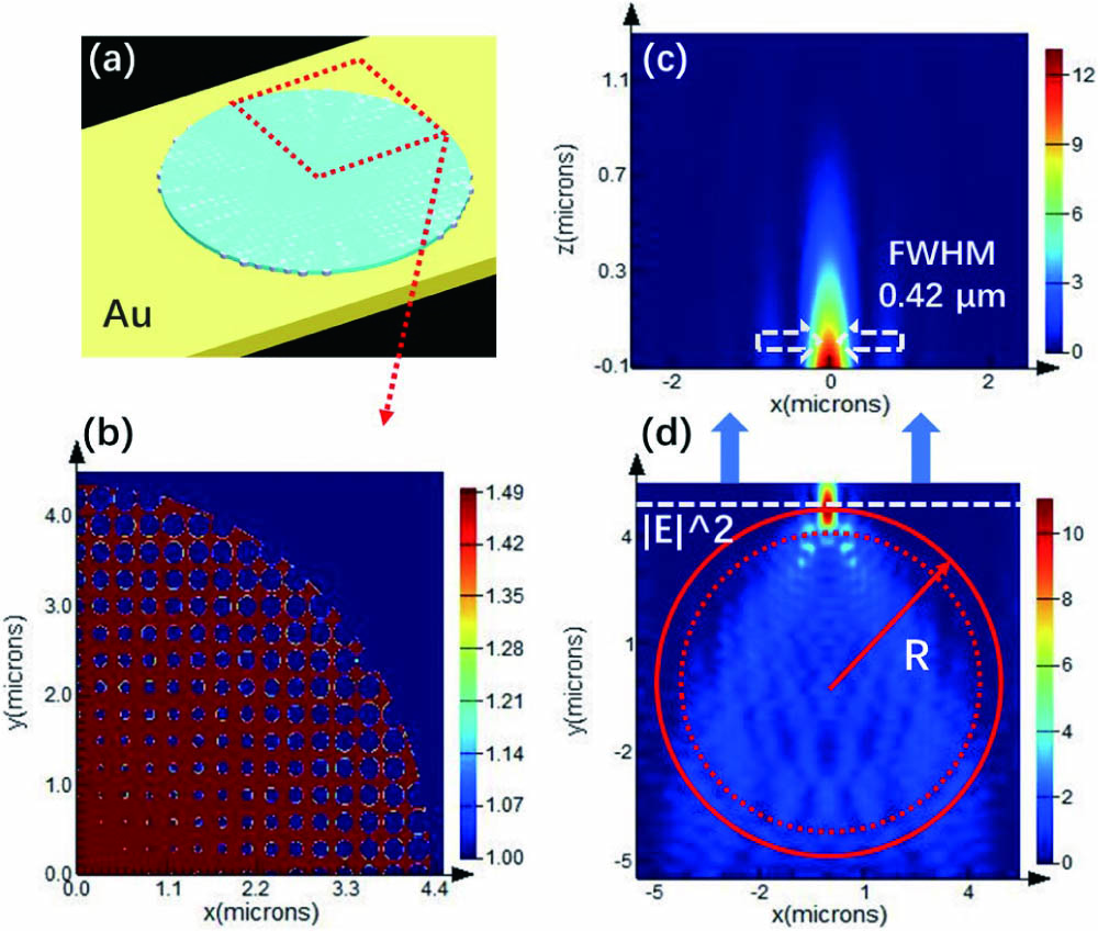
Fig. 2. (a), (c), (e), and (g) Transverse cross sections of the intensity profile at the point ρ=R in the y direction. (b), (d), (f), and (h) Intensity distributions of SPPs (3D simulation) propagating along y direction and passing through the PMLL with different heights. The red circles indicate the radius R of the PMLL. The red dotted circles indicate the real area of the designed lens. The white dotted lines indicate the position y=R.

下载图片 查看原文

Fig. 3. (a) and (e) Schematic diagram for a PMLL. (b) and (f) Quarter enlarged view of the top of the PMMA film with air holes. (c) and (g) Transverse cross section of the intensity profile at the point ρ=R in the y direction. (d) and (h) Intensity distributions of SPPs (3D simulation) propagating along y direction and passing through a PMLL. The red circles indicate the radius R of the PMLL. The red dotted circles indicate the real area of the designed lens. The white dotted lines indicate the position y=R.

下载图片 查看原文

Fig. 4. (a) Schematic diagram for a taper. (b) Schematic diagram for a PMLL coupler. (c) Transverse cross section of the electric field profile at the position y=7μm. (d) Electric field profile of SPPs propagating along y direction, passing through a taper coupler, and coupled to the 40 nm wide waveguide. (e) Transverse cross section of the electric field profile at the position y=7μm. (f) Electric field profile of SPPs propagating along y direction, passing through a PMLL, and coupled to the 40 nm wide waveguide. The red circle indicates the position of the PMLL, and the white dotted line indicates the position of the monitor.

下载图片 查看原文

Fig. 5. The performance of the PMLL coupler and taper coupler based on 3D simulations in a broad bandwidth.

下载图片 查看原文

Lei Zhang, Lin Wang, Yanqing Wu, Renzhong Tai. Plasmonic Luneburg lens and plasmonic nano-coupler[J]. Chinese Optics Letters, 2020, 18(9): 092401.

本文已被 1 篇论文引用
被引统计数据来源于中国光学期刊网
引用该论文: TXT   |   EndNote

相关论文

加载中...

关于本站 Cookie 的使用提示

中国光学期刊网使用基于 cookie 的技术来更好地为您提供各项服务,点击此处了解我们的隐私策略。 如您需继续使用本网站,请您授权我们使用本地 cookie 来保存部分信息。
全站搜索
您最值得信赖的光电行业旗舰网络服务平台!