Author Affiliations
Abstract
1 Department of Electrical Engineering, Stanford University, Stanford, California 94305, USA
2 Department of Materials Science and Engineering, Stanford University, Stanford, California 94305, USA
3 Department of Electrical Engineering, National Taiwan University, Taipei 10617, Taiwan
An efficient monolithically integrated laser on Si remains the missing component to enable Si photonics. We discuss the design and fabrication of suspended and tensile-strained Ge/SiGe multiple quantum well microdisk resonators on Si for laser applications in Si photonics using an all-around SiNx stressor. An etch-stop technique in the Ge/SiGe system is demonstrated and allows the capability of removing the defective buffer layer as well as providing precise thickness control of the resonators. Photoluminescence and Raman spectroscopy indicate that we have achieved a biaxial tensile strain shift as high as 0.88% in the microdisk resonators by adding a high-stress SiNx layer. Optical gain calculations show that high positive net gain can be achieved in Ge quantum wells with 1% external biaxial tensile strain.
(250.5590) Quantum-well -wire and -dot devices (250.5230) Photoluminescence (310.1860) Deposition and fabrication (160.6000) Semiconductor materials. Photonics Research
2017, 5(6): 060000B7

Author Affiliations
Abstract
1 Institute of Optics and Electronics, Chinese Academy of Sciences, Chengdu 610209, China
2 University of Chinese Academy of Sciences, Beijing 100039, China
3 School of Optoelectronic Information, University of Electronic Science and Technology of China, Chengdu 610054, China
To simultaneously obtain high-resolution multi-wavelength (from visible to near infrared) tomographic images of the solar atmosphere, a high-performance multi-wavelength optical filter has to be used in solar imaging telescopes. In this Letter, the fabrication of the multi-wavelength filter for solar tomographic imaging is described in detail. For this filter, Ta2O5 and SiO2 are used as high- and low-index materials, respectively, and the multilayer structure is optimized by commercial Optilayer software at a 7.5° angle of incidence. Experimentally, this multi-wavelength optical filter is prepared by a plasma ion-assisted deposition technique with optimized deposition parameters. High transmittance at 393.3, 396.8, 430.5, 525, 532.4, 656.8, 705.8, 854.2, 1083, and 1565.3 nm, as well as high reflectance at 500 and 589 nm are achieved. Excellent environmental durability, demonstrated via temperature and humidity tests, is also established.
310.0310 Thin films 310.1860 Deposition and fabrication Chinese Optics Letters
2017, 15(12): 123101

Author Affiliations
Abstract
School of Information Science and Engineering, Shandong University, Jinan 250100, China
ZnO films containing Er and Ge nanocrystals (nc-Ge) were synthesized and their photoluminescence (PL) properties were studied. Visible and near-infrared PL intensities are found to be greatly increased in nc-Ge-containing film. Er-related 1.54 μm emission has been investigated under several excitation conditions upon different kinds of Ge, Er codoped ZnO thin films. 1.54 μm PL enhancement accompanied by the appearance of nc-Ge implies a significant correlation between nc-Ge and PL emission of Er3+. The increased intensity of 1.54 μm in Ge:Er:ZnO film is considered to come from the joint effect of the local potential distortion around Er3+ and the possible energy transfer from nc-Ge to Er3+.
(160.2540) Fluorescent and luminescent materials (160.4236) Nanomaterials (160.5690) Rare-earth-doped materials (310.6860) Thin films optical properties (310.1860) Deposition and fabrication. Photonics Research
2017, 5(6): 06000567

Author Affiliations
Abstract
1 School of Materials Science and Engineering, Shanghai University, Shanghai 200444, China
2 CAS Key Laboratory of Materials for Energy Conversion, Shanghai Institute of Ceramics, Chinese Academy of Sciences, Shanghai 200050, China
Molybdenum (Mo) thin films, most commonly used as electrical back contacts in Cu(In,Ga)Se2 (CIGS) solar cells, are deposited by rf and dc magnetron sputtering in identical systems to study the discrepancy and growth mechanisms of the two sputtering techniques. The results reveal that though different techniques generally deposit films with different characteristic properties, Mo films with similar structural and physical properties can be obtained at respective suitable deposition conditions. Highly adhesive and conductive Mo films on soda lime glass are further optimized, and the as-fabricated solar cells reach efficiencies as high as 9.4% and 9.1% without an antireflective layer.
310.1860 Deposition and fabrication 040.5350 Photovoltaic 350.6050 Solar energy Chinese Optics Letters
2016, 14(4): 043101

Author Affiliations
Abstract
State Key Laboratory of Modern Optical Instrumentation, College of Optical Science and Engineering, Zhejiang University, Hangzhou 310027, China
Silicon-rich oxide films with controllable optical constants and properties are deposited by the reactive magnetron sputtering method on a Si target. The O/Si atomic ratio x of SiOx is tuned from 0.12 to 1.84 by adjusting the oxygen flow rate, which is found to be a more effective way to obtain SiOx films compared with changing the oxygen content [O2/(Ar+O2) ratio]. The optical properties of SiOx films can be tuned from semiconductor to dielectric as a function of ratio x. The structures and components are also investigated by an x ray photoelectron spectroscopy analysis of the Si 2p core levels, the results of which exhibit that the structures of SiOx can be thoroughly described by the random bonding model.
160.4670 Optical materials 310.6860 Thin films, optical properties 310.1860 Deposition and fabrication Chinese Optics Letters
2016, 14(5): 051603
Author Affiliations
Abstract
1 Institute of Optics and Electronics, Chinese Academy of Sciences, Chengdu 610209, China
2 University of Chinese Academy of Sciences, Beijing 100039, China
To improve the optical performance of an antireflection (AR) coating on a micro-spherical substrate, the ray angle of the incidence distribution and the thickness profile are taken into consideration during the optical coating design. For a convex spherical substrate with a radius of curvature of 10 mm and a clear aperture of 10 mm, three strategies are used for the optimization of the spectral performance of a broadband AR coating in the spectral region from 480 to 720 nm. By comparing the calculated residual reflectance and spectral uniformity, the developed method demonstrates its superiority in spectral performance optimization of an AR coating on a micro-spherical substrate.
310.0310 Thin films 310.1860 Deposition and fabrication 310.6805 Theory and design Chinese Optics Letters
2016, 14(9): 093101
Author Affiliations
Abstract
1 State Key Laboratory of Advanced Optical Communication Systems and Networks, Department of Electronic Engineering, Shanghai Jiao Tong University, Shanghai 200240, China
2 Key Laboratory of Materials for High-Power Laser, Shanghai Institute of Optics and Fine Mechanics, Chinese Academy of Sciences, Shanghai 201800, China
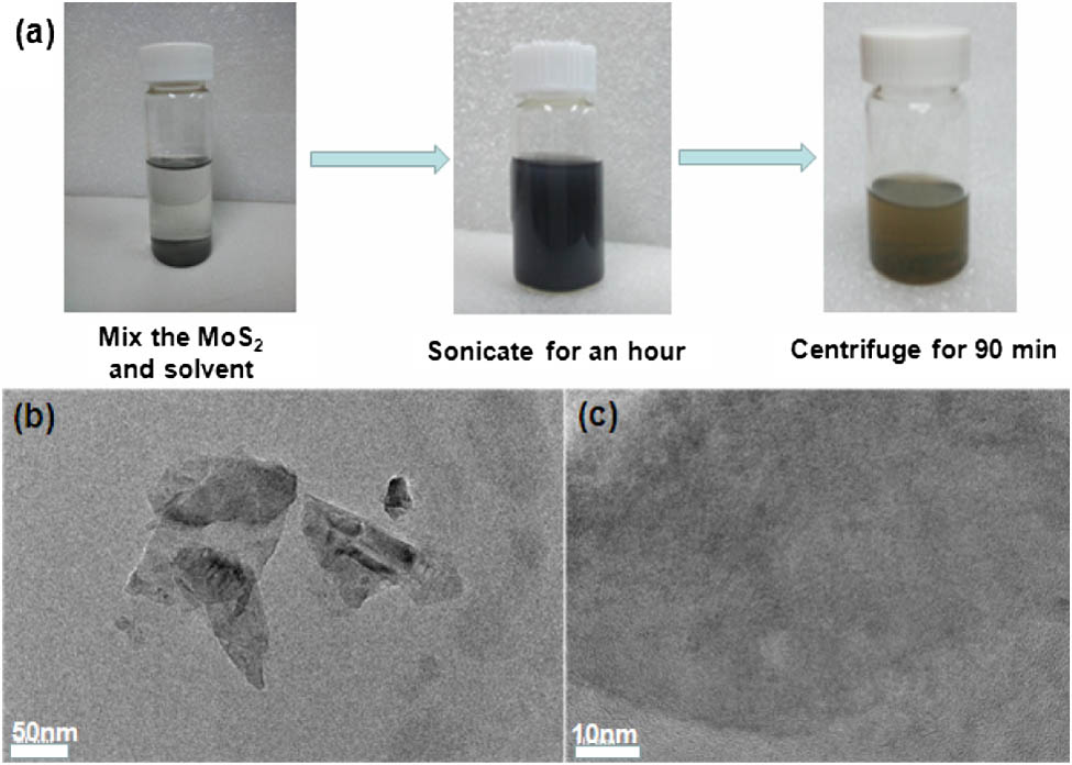
Deposition of two-dimensional (2D) MoS2 materials on the tapered fiber allows various photonic applications including saturable absorbers and four-wave mixing. Ethanol catalytic deposition (ECD) of MoS2 on the optical tapered fiber was proposed and demonstrated in this work. Different from the conventional optical driven deposition using water or organic solvent, the ECD method utilized the high volatility of the ethanol solvent, which significantly increased the movement speed of the MoS2 nanosheets and thus boosted the deposition rate and reduced the minimum power threshold to drive the deposition. We believe the ECD method should be able to be applied to other similar 2D materials such as other types of transition metal chalcogenides.
Nonlinear optical materials Deposition and fabrication Nonlinear optical devices Photonics Research
2015, 3(3): 0300A102

Author Affiliations
Abstract
1 Department of Optical Science and Engineering, Fudan University, Shanghai Ultra-Precision Optical Manufacturing Engineering Center, Shanghai 200433, China
2 Key Laboratory of Micro and Nano Photonic Structures (Ministry of Education), Shanghai 200433, China
3 College of Physical Science and Engineering, Tongji University, Shanghai 200092, China
4 Department of Medical Physics, Weifang Medical University, Shandong 261053, China
A number of zinc oxide (ZnO) films are deposited on silicon substrates using the magnetron sputtering method. After undergoing thermal treatment under different conditions, those films exhibit hexagonal wurtzite structures and different photoluminescent characteristics. Besides the notable ultraviolet emission, which is related to the free exciton effect, a distinct blue fluorescence around 475 nm is found in some special samples. The blue photoluminescence emission of the ZnO film is believed to be caused by oxygen vacancies.
310.6860 Thin films, optical properties 310.1860 Deposition and fabrication 300.6280 Spectroscopy, fluorescence and luminescence 260.3800 Luminescence Chinese Optics Letters
2015, 13(10): 103101
Author Affiliations
Abstract
In conventional pulsed laser deposition (PLD) technique, plume deflection and composition distribution change with the laser incident direction and pulse energy, then causing uneven film thickness and composition distribution for a multicomponent film and eventually leading to low device quality and low rate of final products. We present a novel method based on PLD for depositing large CIGS films with uniform thickness and stoichiometry. By oscillating a mirror placed coaxially with the incident laser beam, the laser's focus is scanned across the rotating target surface. This arrangement maintains a constant reflectance and optical distance, ensuring that a consistent energy density is delivered to the target surface by each laser pulse. Scanning the laser spot across the target suppresses the formation of micro-columns, and thus the plume deflection effect that reduces film uniformity in conventional PLD technique is eliminated. This coaxial scanning PLD method is used to deposit a CIGS film, 500 nm thick, with thickness uniformity exceeding ±3% within a 5 cm diameter, and exhibiting a highly homogeneous elemental distribution.
220.0220 Optical design and fabrication 220.4830 Systems design 310.0310 Thin films 310.1860 Deposition and fabrication Chinese Optics Letters
2014, 12(7): 072201
Author Affiliations
Abstract
A model is developed to improve thickness uniformity of coatings on spherical substrates rapidly and automatically using fixed shadow masks in a planetary rotation system. The coating thickness is accurately represented by a function composed of basic thickness, self-shadow effect, and shadow mask function. A type of mask with parabolic contours is proposed, and the thickness uniformity of coatings on spherical substrates can be improved in a large range of ratios of clear aperture (CA) to radius of curvature (RoC) by optimizing shadow masks using a numerical optimization algorithm. Theoretically, the thickness uniformity improves to more than 97.5% of CA/RoC from –1.9 to 1.9. Experimentally, the thickness uniformities of coatings on a convex spherical substrate (CA/RoC = 1.53) and on a concave spherical substrate (CA/RoC=–1.65) improve to be better than 98.5% after corrected by the shadow masks.
310.0310 Thin films 310.6805 Theory and design 310.1860 Deposition and fabrication Chinese Optics Letters
2014, 12(5): 053101


