1 河北工程大学信息与电气工程学院,河北 邯郸 056038
2 河北工程大学数理科学与工程学院,河北 邯郸 056038
基于导模共振光栅的集成光学滤波器在光纤通信中具有潜在的应用前景,然而单个导模共振光栅的输出光谱一般呈现洛伦兹线型,这会阻碍该类结构在波分复用系统中的应用。传统方法一般采用多个谐振腔级联的方式实现平顶滤波响应,然而整个结构的体积较大,制作工艺较为复杂,因此提出一种基于级联双层导模共振光栅结构,其输出光谱响应为平顶陡边型。首先建立器件的物理模型,其物理机理是将导模共振效应与法布里-珀罗谐振效应结合,然后利用物理模型分析和设计滤波器结构。研究发现该滤波器的中心波长为1550 nm,其3 dB带宽可以增加至20 nm。
光栅 波长滤波器 导模共振 法布里-珀罗谐振腔 平顶光谱 激光与光电子学进展
2021, 58(11): 1105001

Author Affiliations
Abstract
1 Department of Electronic Engineering, Kwangwoon University, Seoul 01897, South Korea
2 Laser Physics Centre, Research School of Physics and Engineering, Australian National University, Canberra ACT 0200, Australia
3 College of Information Science and Technology, Jinan University, Guangzhou 510632, China
Angle tolerant transmissive subtractive color filters incorporating a metasurface exploiting hydrogenated amorphous silicon nanopillars (NPs) on a glass substrate were proposed and demonstrated. The achieved transmission efficiency ranged from 75% to 95% at off-resonance wavelengths. For an NP resonator, electric and magnetic-field distributions in conjunction with absorption cross-sections were investigated to confirm a resonant transmission dip, which is primarily governed by the absorption resulting from simultaneous excitation of magnetic and electric dipoles via Mie scattering. The proposed devices exhibit higher angular tolerance and lower crosstalk for the absorption spectra and, therefore, are applicable with photodetectors, image sensors, and imaging/display devices.
230.7408 Wavelength filtering devices 230.0040 Detectors Chinese Optics Letters
2019, 17(8): 082301

Author Affiliations
Abstract
1 National Laboratory for Optoelectronics, School of Optical and Electronic Information, Huazhong University of Science and Technology, Wuhan 430074, China
2 Department of Photonics Engineering, Technical University of Denmark, 2800 Kgs. Lyngby, Denmark
Tunable optical delay lines are one of the key building blocks in optical communication and microwave systems. In this work, tunable optical delay lines based on integrated grating-assisted contradirectional couplers are proposed and experimentally demonstrated. The device performance is comprehensively improved in terms of parameter optimization, apodization analysis, and electrode design. Tunable group delay lines of 50 ps at different wavelengths within the bandwidth of 12 nm are realized with a grating length of 1.8 mm. Under thermal tuning mode, the actual delay tuning range is around 20 ps at 7.2 V voltage. At last, a new scheme adopting an ultra-compact reflector for doubling group delay is proposed and verified, achieving a large group delay line of 400 ps and a large dispersion value up to 5.5×10⁶ ps/(nm·km) within bandwidth of 12 nm. Under thermal tuning mode, the actual delay tuning range is around 100 ps at 8 V voltage.
Integrated optics devices Wavelength filtering devices Optical buffers Photonics Research
2018, 6(9): 09000880
Author Affiliations
Abstract
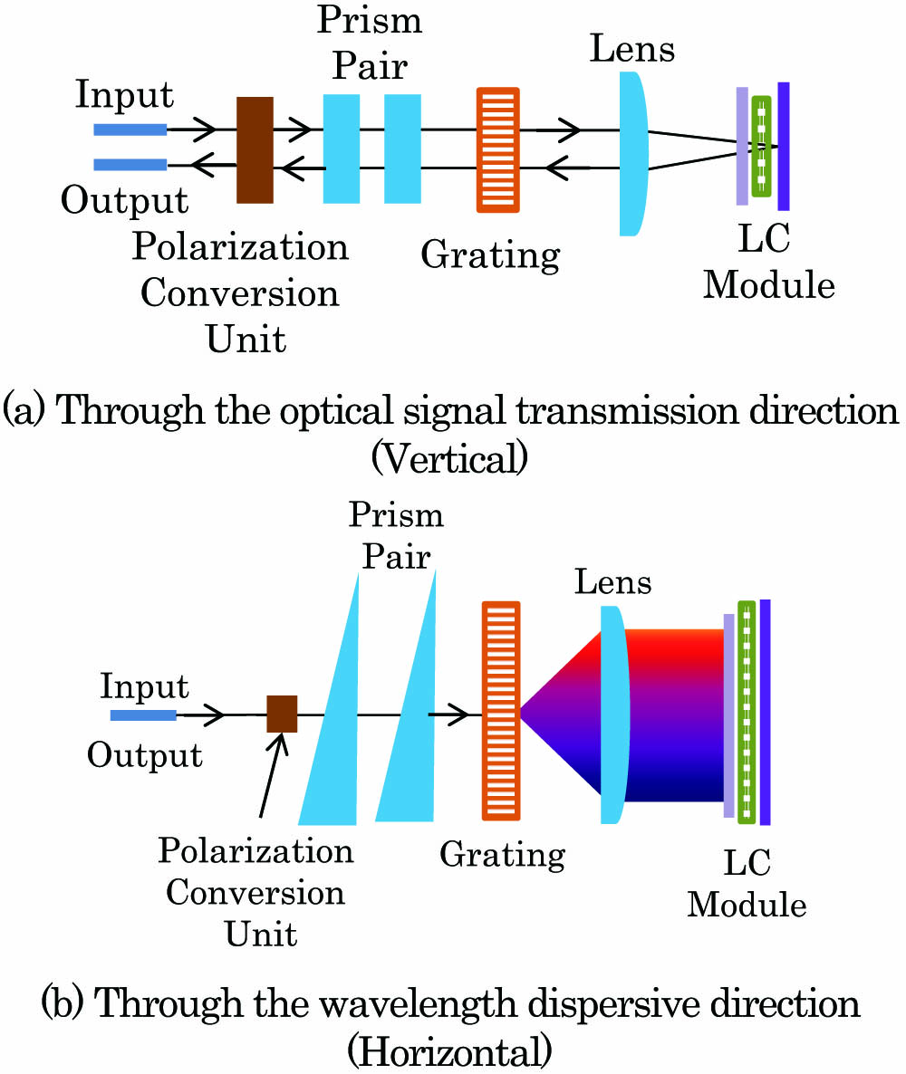
1 Wuhan National Lab for Optoelectrics, Huazhong University of Science and Technology, Wuhan 430074, China
2 Accelink Technologies Co., Ltd., Wuhan 430205, China
A bandwidth-tunable optical passband filter with tunable attenuation is proposed. The filter, composed of a transmission liquid crystal array and high-resolution diffraction grating, was successfully demonstrated based on the compact spatial light design. Experimental results showed that the bandwidth, wavelength, and attenuation could be tuned by controlling the voltage applied on the liquid crystal array. The insertion loss was less than 3 dB; the attenuation tuning range was from 0 to 15 dB. The bandwidth tuning range was from 50 to 5000 GHz, which covered the full C band. The filter can meet the technical requirements of colorless-directionless-contentionless-flexible reconfigurable optical add/drop multiplexer.
060.2605 Free-space optical communication 130.7408 Wavelength filtering devices Chinese Optics Letters
2018, 16(7): 070602

Author Affiliations
Abstract
1 Image Processing Systems Institute—Branch of the Federal Scientific Research Centre “Crystallography and Photonics” of Russian Academy of Sciences, 151 Molodogvardeyskaya St., Samara 443001, Russia
2 Samara National Research University, 34 Moskovskoe Shosse, Samara 443086, Russia
We propose a simple integrated narrowband filter consisting of two grooves on the surface of a slab waveguide. Spectral filtering is performed in transmission at oblique incidence due to excitation of an eigenmode of the structure localized at a ridge cavity between the grooves. For the considered parameters, zero reflectance and unity transmittance are achieved at resonant conditions. The width and location of the transmittance peak can be controlled by changing the widths of the grooves and of the ridge, respectively. The proposed filter may find application in waveguide-integrated spectrometers.
Wavelength filtering devices Microcavity devices Integrated optics devices Guided waves Resonance domain Subwavelength structures Photonics Research
2018, 6(1): 01000061

Author Affiliations
Abstract
School of Optical and Electrical Information, Huazhong University of Science and Technology, Wuhan 430074, China
With the rapidly increasing bandwidth requirements of optical communication networks, compact and low-cost large-scale optical switches become necessary. Silicon photonics is a promising technology due to its small footprint, cost competitiveness, and high bandwidth density. In this paper, we demonstrate a 12×12 silicon wavelength routing switch employing cascaded arrayed waveguide gratings (AWGs) connected by a silicon waveguide interconnection network on a single chip. We optimize the connecting strategy of the crossing structure to reduce the switch’s footprint. We develop an algorithm based on minimum standard deviation to minimize the port-to-port insertion loss (IL) fluctuation of the switch globally. The simulated port-to-port IL fluctuation decreases by about 3 dB compared with that of the conventional one. The average measured port-to-port IL is 13.03 dB, with a standard deviation of 0.78 dB and a fluctuation of 2.39 dB. The device can be used for wide applications in core networks and data centers.
Networks, wavelength routing Integrated optics devices Wavelength filtering devices Photonics Research
2018, 6(5): 05000380

Author Affiliations
Abstract
1 Wuhan National Laboratory for Optoelectronics, Huazhong University of Science and Technology, Wuhan 430074, China
2 e-mail: huangqz@mail.hust.edu.cn
3 e-mail: jsxia@hust.edu.cn
We have designed and realized an athermal 4-channel wavelength (de-)multiplexer in silicon nitride (SiN). Minimized thermal sensitivity is achieved in a wide wavelength range by using wide and narrow waveguides with low and different thermal-optic coefficients in the two arms of Mach–Zehnder interferometers (MZIs). The SiN core layer and SiO2 cladding layers are deposited by a low-temperature plasma-enhanced chemical vapor deposition process. The fabricated MZI filter exhibits a thermal sensitivity within ±2.0 pm/°C in a wavelength range of 55 nm to near 1300 nm. Then, an athermal (de-)multiplexer based on cascaded MZIs has been demonstrated with a crosstalk ≤ 22 dB and a thermal sensitivity <4.8 pm/°C for all four channels, reduced by 77% compared to a conventional SiN (de-)multiplexer. Owing to the passive operation and compatibility with the CMOS backend process, our devices have potential applications in 3D integration of photonics and electronics.
Integrated optics devices Wavelength filtering devices Photonics Research
2018, 6(7): 07000686

Author Affiliations
Abstract
1 Photonics Research Group, Ghent University-IMEC, Department of Information Technology, Ghent University, Ghent 9052, Belgium
2 Center for Nano- and Biophotonics, Ghent University, Ghent 9052, Belgium
In this paper, we theoretically propose and experimentally demonstrate the manipulation of a novel degree of freedom in ring resonators, which is the coupling from the clockwise input to the counterclockwise propagating mode (and vice versa). We name this mechanism backcoupling, in contrast with the normal forward-coupling of a directional coupler. It is well known that internal reflections will cause peak splitting in a ring resonator. Our previous research demonstrated that the peak asymmetry will be strongly influenced by the backcoupling. Thus, it is worth manipulating the backcoupling in order to gain full control of a split resonance for the benefit of various resonance-splitting-based applications. While it is difficult to directly manipulate the backcoupling of a conventional directional coupler, here we design a circuit explicitly for manipulating the backcoupling. It can be potentially developed for applications such as single sideband filter, resonance splitting elimination, Fano resonance, and ultrahigh-Q and finesse.
Integrated optics devices Resonators Wavelength filtering devices Traveling-wave devices Electromagnetic optics Photonics Research
2018, 6(6): 06000620

Author Affiliations
Abstract
1 IDLab, Department of Information Technology, Ghent University-imec, Ghent, Belgium
2 Photonics Research Group, Department of Information Technology, Ghent University-imec, Ghent, Belgium
In this paper, a novel modeling and simulation method for general linear, time-invariant, passive photonic devices and circuits is proposed. This technique, starting from the scattering parameters of the photonic system under study, builds a baseband equivalent state-space model that splits the optical carrier frequency and operates at baseband, thereby significantly reducing the modeling and simulation complexity without losing accuracy. Indeed, it is possible to analytically reconstruct the port signals of the photonic system under study starting from the time-domain simulation of the corresponding baseband equivalent model. However, such equivalent models are complex-valued systems and, in this scenario, the conventional passivity constraints are not applicable anymore. Hence, the passivity constraints for scattering parameters and state-space models of baseband equivalent systems are presented, which are essential for time-domain simulations. Three suitable examples demonstrate the feasibility, accuracy, and efficiency of the proposed method.
Wavelength filtering devices Systems design Photonic integrated circuits Photonics Research
2018, 6(6): 06000560
Author Affiliations
Abstract
Wuhan National Laboratory for Optoelectronics, School of Optical and Electronic Information, Huazhong University of Science and Technology, 430074, Wuhan, China
All-optical integrators are key devices for the realization of ultra-fast passive photonic networks, and, despite their broad applicability range (e.g., photonic bit counting, optical memory units, analogue computing, etc.), their realization in an integrated form is still a challenge. In this work, an all-optical integrator based on a silicon photonic phase-shifted Bragg grating is proposed and experimentally demonstrated, which shows a wide operation bandwidth of 750 GHz and integration time window of 9 ps. The integral operation for single pulse, in-phase pulses, and π-shifted pulses with different delays has been successfully achieved.
Integrated optics devices Wavelength filtering devices Analog optical signal processing All-optical devices Photonics Research
2017, 5(3): 03000182


