Graphene-empowered dynamic metasurfaces and metadevices  Download: 1290次
1 Introduction
Metasurfaces, artificial subwavelength structured interfaces, exhibit unprecedented capabilities to manipulate electromagnetic (EM) waves ranging from visible to terahertz (THz) and microwave frequencies1-8. By precisely managing the geometric size, orientation, and arrangement of each metaatom in metasurfaces, one can control the amplitude, phase, polarization, and/or frequency of EM waves on demand9-14. In the past decade, this fascinating area has undergone rapid developments, and a plethora of advanced metadevices with outstanding functionalities have been exploited including diffraction-limited focusing15-21, holography22-26, structured light generation27-29, orbital-angular momentum multiplexing/demultiplexing30, 31, and dispersion engineering32-35. It is noteworthy that besides the intriguing functionalities, the natural instinct to miniaturize traditional devices and systems is the ultimate motive force to the development of metasurfaces and metadevices in terms of engineering and industrial applications36. In pace with increasingly powerful micro/nano-fabrication technologies37-41, various functionalized metasurfaces have been integrated on fiber facets42, and into semiconductor43, solid-state44 as well as fiber lasers45, infusing new life and capabilities into the traditional nanodevices. Currently, multi-functional and multi-dimensional metasurfaces are arousing a period of revolution in both traditional and emerging application fields46-48, such as integrated photonics49, 50, nonlinear optics51, 52, next-generation communications53, 54, artificial intelligences55, 56, and quantum technologies57, 58.
Due to the passive nature of building blocks in general made of metals and/or dielectrics, however, aforementioned metasurfaces and metadevices mainly work at static, which means their functionalities cannot be actively tuned in situ after fabrication. There is no doubt, such static feature leads to a fall-off in the functionality of dynamical manipulations and seriously impedes their application scenarios, where dynamic EM wave manipulations are highly desired59-63, for example, varifocal lens64, dynamic holography65, and beam steering in LiDAR system66. Motivated by those significant requirements, scientists have struggled for years to improve the dynamical tunability of metasurfaces, and introducing active materials or components into the passive metasurfaces has been proposed as the first thought strategy. Up to now, various active materials and components such as transparent conducting oxides67-69, phase-change materials70-73, 2D materials (particularly graphene)74-79, varactor diodes80-83, elastic materials84-86, and micro-electro-mechanical system87-89, have been demonstrated theoretically and experimentally to empower the active tunability to metasurfaces and metadevices by applying external thermal, electrical, optical, and mechanical stimulus, giving rise to a new direction, i.e., dynamic (e.g. tunable, reconfigurable, programable, intelligent, and digital coding) metasurfaces and metadevices90-96. It should be noted that although previous researches provide a major source of inspiration for dynamic metasurfaces and metadevices, each type of active materials and components holds a set of unique characteristics, provides encouraging opportunities, and also suffers from different limitations as well as challenges. Several excellent review articles published in recent years have focused on this area to discuss the aforementioned issues97-101. However, a comprehensive review on graphene-based dynamic metasurfaces and metadevices is still absent, which are of equal and even more significance due to the extraordinary properties of graphene.
Recent years have witnessed the explosive developments of 2D materials-based electronics and photonics with increasing maturity of preparation and fabrication techniques102-115. Although the family of 2D materials goes from strength to strength, graphene is recognized all the time as one of the most powerful 2D materials due to its intrinsic advantages of active tunability by external stimulus (especially by electrical basis)116, enhanced wave-matter interactions117, ultrabroadband response118, and CMOS-compatibility113. Currently, the combination of the two exciting research fields, i.e., 2D materials and metasurfaces, is propelling the metasurfaces and metadevices to new heights: multifunctionality together with tunability. Thereinto, graphene has been so far the most attractive candidate to exploit dynamic metasurfaces and metadevices with different mechanisms, configurations, and functionalities in the mid-infrared (MIR), THz, and microwave regimes, which can be categorized into two classes: metasurfaces with building blocks of structured graphene and hybrid metasurfaces integrated with graphene74-79, 119-127. The former is called graphene plasmonic metasurfaces and the latter graphene-hybrid metasurfaces (as shown in

Fig. 1. Overview of state-of-the-art selected functionalities of dynamic metasurfaces and metadevices empowered by graphene. According to the different operation mechanisms, graphene-empowered dynamic metasurfaces are here divided into two classes: graphene plasmonic metasurfaces and graphene-hybrid metasurfaces, each of which holds half the sky. The abbreviations of G and Meta represent graphene and metasurface, and the symbols of A, φ, P, and f stand for the amplitude, phase, polarization, and frequency of EM waves respectively.
2 Fundamentals of graphene
In 2004, Novoselov and Geim et al. successfully prepared the single-layer graphene from highly oriented pyrolytic graphite by mechanical exfoliation and demonstrated a field-effect transistor using high-quality few-layer graphene, which lifted the curtain of research on 2D materials128-131. The Nobel Prize for Physics in 2010 publicized widely this powerful one-atomic-thick material and also the simple preparation method of mechanical exfoliation, providing the easy access to prepare high-quality graphene, which is now the most popular method, particularly in the photonics and optoelectronics. Since then, 2D materials with the structure and properties similar to graphene, such as black phosphorus (BP)132-134 and transition metal dichalcogenides (TMDCs)135-137, began to gather increasing attention of scientists in the multidisciplinary field, especially in the photonic and optoelectronic community due to their exceptional electrical and optical properties108, 138. Although the family of 2D materials is rather plentiful, due to the easy preparation of remarkably high-quality graphene, flexibly electrical tunability, and CMOS-compatible with silicon photonics, graphene is still one of the most powerful 2D materials for developing high-performance nanodevices including metadevices, where the qualities of 2D materials are critically important, for instance, the mobility, conductivity, defect, size, and layer number114, 139, 140. In this Section, we centre upon graphene to discuss its basic material properties and plasmon mode, and provide the theoretical and numerical models of graphene plasmons. It should be noted that graphene in general represents the single-layer graphene throughout this review if there is no special description.
2.2 Basic material properties of graphene
It is well-known that due to its unique electronic structure, graphene has been hailed as a wonderful material with distinctive properties, which provide new solutions to integrated electronics and photonics with the compact footprint, remarkably electrical tunability, broadband and high-speed operation.
(i) One-atomic-scale thickness. Graphene is a single-layer atomic crystal of hexagonally-arranged sp2-hybridized carbon atoms with the lattice constant of ~0.142 nm128. As shown in
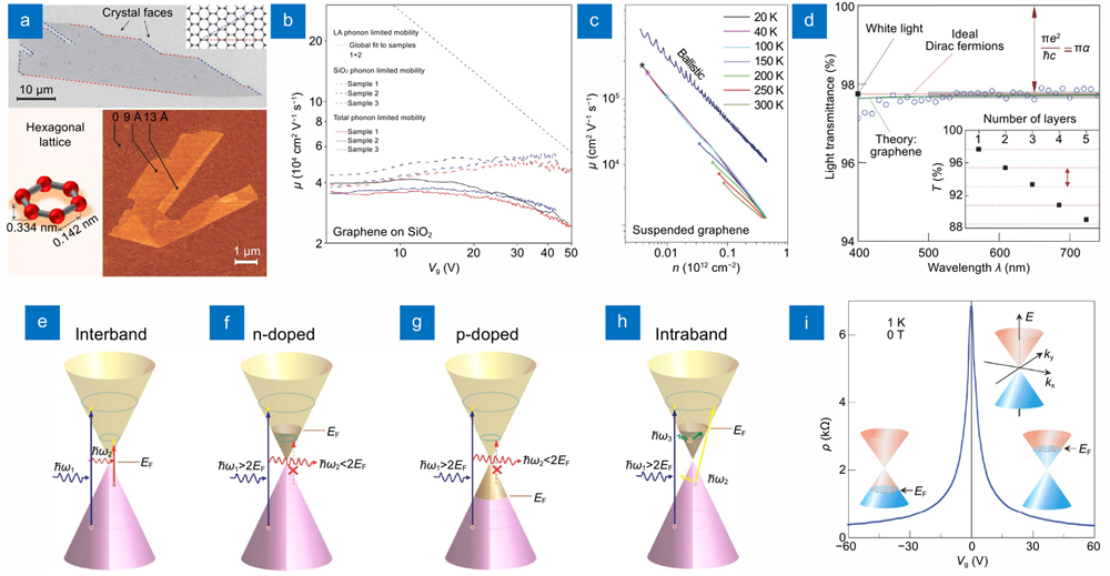
Fig. 2. The basic material properties of graphene. (a ) Micrographs of the scanning electron microscopy (upper panel) and atomic force microscopy (lower right panel), and also a schematic diagram of the 2D hexagonal lattice of graphene (lower left panel). Typical carrier mobility for (b ) graphene on SiO2 with gate-voltage dependence at room temperature and (c ) suspended graphene depending on carrier density at the different temperatures. (d ) Measured transmission spectrum of graphene in the visible range, where the inset is the transmittance as a function of the number of graphene layers. The band structures and its possible transition process for: (e ) pristine or undoped, (f ) n-doped, (g ) p-doped graphene, and (h ) plasmon absorption in n-doped graphene. (i ) Dynamic resistivity ρ with gate voltage Vg applied on graphene, in which the insets show the corresponding position of the Fermi energy EF with changing Vg. Figure reproduced with permission from: (a, i) ref.130, © 2007 Springer Nature; (b) ref.142, © 2008 Springer Nature; (c) ref.144, © 2008 Springer Nature; (d) ref.151, © 2008 AAAS; (e–h) ref.118, © 2012 ACS.
(ii) Ultra-high intrinsic carrier mobility. The linear energy-momentum dispersion near the Dirac point renders electrons in graphene travelling at a constant velocity of 3×10⁶ m/s (only 100 times smaller than the light speed, defined as the Fermi velocity), which means the carrier mobility can be ultra-high and thus graphene is an excellent conductor of electricity. It should be pointed out that the mobility can also remain high even when the carrier density is zero at the Dirac point, which is quietly different from semiconductors where carriers become immobile at low density. Although the environment (particular the substrate) significantly affects the mobility of graphene in practice, the experimentally measured mobility is still high enough, for example, ~4×104 cm2V−1s−1 on SiO2 substrate (
(iii) Tunable and broadband responses. Due to the unique electronic band structure that conic-shaped conduction band and valence band meet at the Dirac point, the optical conductance of pristine graphene is frequency-independent and only determined by its fine-structure constant α=e2/ћc≈1/137 (here e is the electron charge, ћ the reduced Planck’s constant, and c the light speed in the vacuum), which directly results in a frequency-independent optical absorption A=πα~2.3% for single-layer graphene and A=Nπα for N-layer graphene, as shown in
The EM response of graphene can be described and determined by its complex conductivity. From this perspective, here the origin of above-discussed dynamic response of graphene is enquired. The surface conductivity of graphene σ can be strictly expressed using the Kubo formula with intraband and interband contributions (σ=σintra+σinter)162-164. Under the random-phase approximation, it can be simplified as,
where e is the electron charge, kB is the Boltzmann constant, T is the temperature, ћ is the reduced Planck’s constant, τ=μEF/(eνF2) is the carrier relaxation lifetime associated with intraband transitions, μ is the carrier mobility, νF=108 cm/s is the Fermi velocity. It is obvious that both intraband and interband conductivities are closely related to the Fermi energy EF determined by the carrier density n=(EF/ћω)2/π, which can be controlled by chemical, magnetical, or electrical doping, indicating that the ultimate tunability of graphene results from its dynamic conductivity. By analyzing the above equations, it is concluded that in the MIR~THz regime, interband conductivity can be ignored and only intraband conductivity need to be considered when ћω<2EF, while in the visible~NIR regime, the interband conductivity dominates. This coincides well with the optical transition process in
It can be seen that
2.3 Plasmons in graphene
Different from photonic modes in dielectrics, there exist special EM modes at the interface of two materials with opposite signs of permittivity (for example, dielectric and conductor), called polaritons, which provide an extraordinary route to manipulate and harness light field below the diffraction limit171-173. In 2D materials, the polaritons can be clarified as plasmon polaritons174, phonon polaritons175, and exciton polaritons176. It is essential that to support and confine these polaritons at an interface, the real part of the permittivity of materials should be negative. As illustrated in
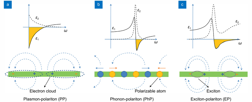
Fig. 3. Polaritons in 2D materials with different dielectric functions and electric field line distributions. (a ) Plasmon-polariton, (b ) phonon-polariton, and (c ) exciton-polariton. The symbol ε1 represents the real part of permittivity, ε2 imaginary part, and ω angular frequency of light. Figure reproduced with permission from ref.171, © 2017 Springer Nature.
In fact, the plasmon polaritons bounded at the interface of a metal and a dielectric is as well-known as surface plasmon polaritons when coupled with photons, by which the important field of plasmonics was established in the last century and has derived straightforwardly the emerging field of nanophotonics181-184. Over the last few decades, a lot of interesting effects, phenomena, and advanced nanophotonic devices based on plasmons have been discovered including metasurfaces and metadevices using noble metals (e.g. gold and silver)185-193. In the ongoing search for alternative plasmonic materials, graphene emerged as a promising one for the MIR and THz applications. Currently, the development of graphene plasmonics is pushing forward the nanophotonics to the longwave infrared and be more powerful194-198. Compared with metallic plasmons, graphene plasmons (GPs) show several advantages. The first and most important is that the carrier density tunability of graphene by various external stimulus enables the flexibly tunable plasmon properties and active devices. Second, GPs can be excited and sustained from THz to MIR frequencies, where metallic plasmons suffer from larger losses, due to the small carrier density of graphene typically less than one percent of gold199, 200. Third, GPs possess extremely strong field confinement together with relatively long propagation distance because of its 2D nature and high carrier mobility. The trade-off between the field confinement and propagation length is universal. To achieve a large propagation length of GPs, increasing the doping density is a direct route, which in turns decreases the confinement. Even for very high-level doping, however, the penetration depth is still a few orders smaller than that of silver, indicating an appropriate balance of the trade-off and the advantage of field confinement under sufficient propagation length201-204.
Similarly, GPs can be divided into propagating and localized modes according to their propagation conditions. Although it has been predicted theoretically that graphene supports plasmons, their exciting and detecting have remained a long-term challenge due to the large momentum mismatch between GPs and free-space photons163, 164, 205. In 2011, Ju et al. successfully excited GPs by coupling incident photons with dipolar plasmon resonances in artificially structured graphene and demonstrated the first graphene metamaterial for tunable THz filters177. As shown in
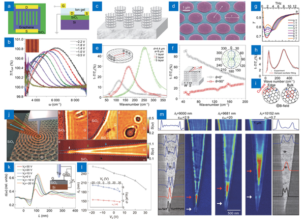
Fig. 4. The pioneering experiments on GPs. Tunable THz metamaterials based on the gated graphene microribbon array: (a ) top-view and side-view illustrations of a typical graphene microribbon array on a Si/SiO2 substrate with ion-gel top gate, (b ) transmission spectra of a graphene microribbon array as gate voltage (the inset: AFM image). Tunable infrared plasmonic devices using the stacked graphene/insulator array: (c ) schematic diagram and (d ) SEM image of the stacked graphene/insulator microdisk array, (e ) extinction spectra for different layer numbers of disks, (f ) extinction spectra of a tunable THz linear polarizer using a stacked graphene/insulator microribbon array. (g ) Transmission spectra of graphene on SiC substrate with defects under different magnetic fields. (h ) Extinction spectrum of the edge and bulk plasmon modes and (i ) their corresponding illustration of charged carrier motions. Real-space imaging of GPs: (j ) diagram of infrared nano-imaging experiment and images of plasmon field amplitude, (k ) field amplitude perpendicular to the graphene edge and (l ) plasmon wavelength as the function of gate voltage (the inset: back-gate bias set-up), (m ) near-field optical images of graphene ribbon and tapered graphene ribbon with different wavelengths of excitation light. Figure reproduced with permission from: (a, b) ref.177, © 2011 Springer Nature; (c–f) ref.206, © 2012 Springer Nature; (g) ref.207, © 2012 ACS; (h, i) ref.208, © 2012 ACS; (j–l) ref.210, © 2012 Springer Nature; (m) ref.209, © 2012 Springer Nature.
2.4 Theoretical and numerical models of GPs
At the same time, a number of theoretical and numerical researchers have predicted that graphene can serve as the outstanding platform for guiding and manipulating energy flow in the 2D and 3D spaces with the assistance of GPs211-222. Here, in order to provide the fundamentals for Sections Metasurfaces with building blocks of structured graphene and Hybrid metasurfaces integrated with graphene, the theoretical and numerical models for propagating GPs in continuous graphene sheets and localized GPs in structured graphene are discussed in details. This Section not only provides a powerful methodology to build the graphene metasurfaces but also can promote a deep understanding of the physics in GPs, which is essential to developing accurate models of metasurfaces and metadevices before experiments. As shown in

Fig. 5. Schematic diagrams of a dielectric-graphene-dielectric waveguide and the EM components of the possible TM as well as TE GP modes. β denotes the propagation constant of GPs, ε1 and ε2 represent the relative permittivity of dielectrics below and above graphene sheet, respectively.
To implement the theoretical analyses based on the Maxwell equations, graphene sheet is regarded as a conducting interface without thickness, and therefore the surface current
According to the wave equations of EM field, the dispersion relation of TM GPs is then derived,
here, wavevectors in dielectrics satisfy
For TE modes, similarly, the boundary condition is (z=0),
The dispersion relation of TE GPs is obtained,
In simulations, graphene sheet is generally regarded as an ultrasmall-thickness (Δ) material with equivalent complex permittivity to represent its material property223-225. The volume conductivity σg,V and volume current density
Assuming the average permittivity of surrounding dielectrics as εd, the Maxwell equations are,
Therefore, the equivalent permittivity of Δ-thickness graphene sheet is expressed as,
It is found that Re(εg) = εd − Im(σg)/(ε0ωΔ) ≈ − Im(σg)/(ε0ωΔ) and Im(εg) = Re(σg)/(ε0ωΔ), which implies that the sign of real (imaginary) part of equivalent permittivity is determined by the sign of imaginary (real) part of surface conductivity. Noteworthy, the sign of Im(σg) plays a crucial role in whether graphene supports TE or TM GP mode, which depends on the Fermi energy of graphene.
For theΔ-thickness graphene model, when Im(σg)<0 (the interband contribution for conductivity is dominant at low Fermi energy), the TE mode is supported and its dispersion relation is226,
Substituting
here Z0=1/(ε0c)=µ0c=377 Ω is the vacuum impedance.
When Im(σg)>0 (the intraband contribution becomes dominant at relatively high Fermi energy,ћω<2EF), the TM mode is supported and its dispersion relation is227,
By the same processing method, the dispersion of TM GPs is reduced to,
It is obvious that,
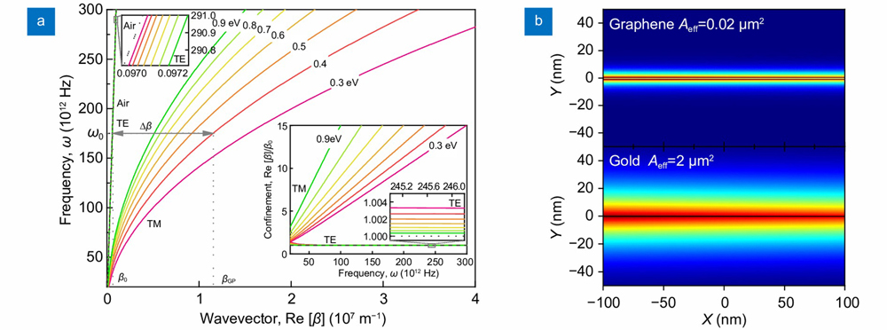
Fig. 6. Fundamental properties of TM and TE GPs in an air-graphene-air waveguide. (a ) Dispersion relation and field confinement of TM and TE GPs as the function of Fermi energy calculated from Eqs. (12) and (14) in the MIR~THz regime. (b ) Field confinement comparison between graphene and gold waveguide using the model in Fig. 5 with the same geometric parameters.
Therefore, to manipulate the energy flow of GPs propagating along with graphene sheet, it is critical to control the propagation conditions as described by
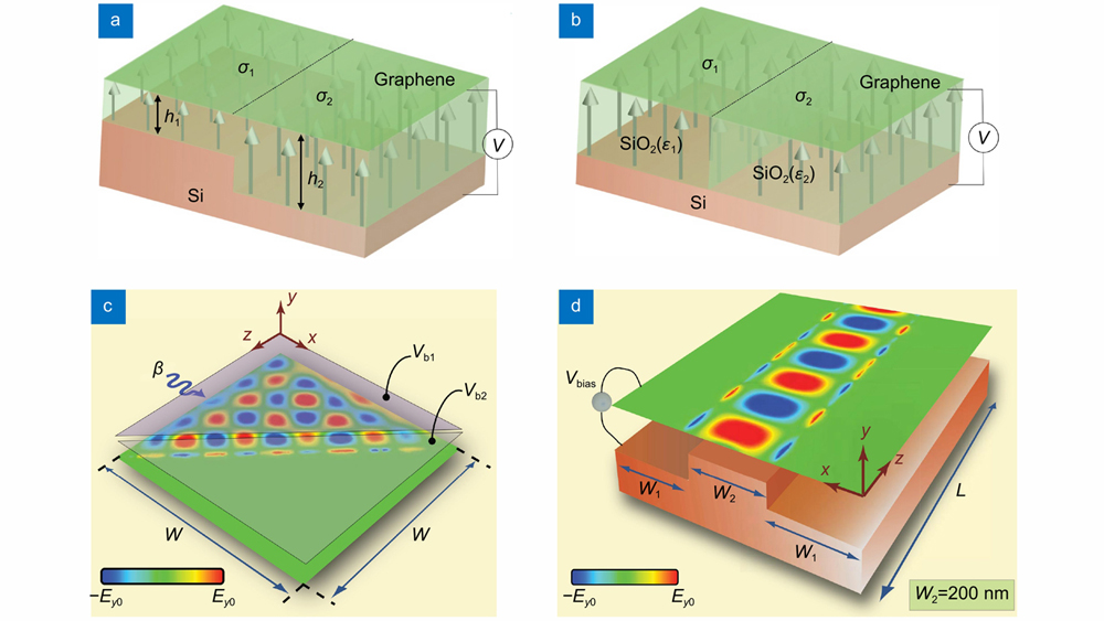
Fig. 7. Theoretical models and numerical results for manipulating the energy flow of propagating GPs on 2D plane of graphene sheet by spatially modulating the surface conductivity of graphene. Schematic diagram of the parallel capacitor model with (a ) uneven ground plate Si (h1≠h2) and (b ) nonuniform spacer for example differently doped SiO2 (ε1≠ε2). (c ) Simulated propagation of GPs on a graphene sheet with different bias voltages (Vb1 corresponds to Im(σg)>0 andVb2 corresponds to Im(σg)<0). (d ) Simulated results of graphene-based 2D waveguide using the model in (a). Figure reproduced with permission from: (c, d) ref.211, © 2011 AAAS.
Compared with the launching difficulty of propagating GPs, structured graphene provides an efficient route to avoid the large momentum mismatch between GPs and excitation light by plasmon resonances, usually termed the localized GP mode177, 206. As discussed in Section Basic material properties of graphene, the surface conductivity of a continuous graphene sheet is described by
where f is the filling factor (the ratio of graphene area to total area), D=e2EF/ћ2 is the Drude weight, and
here εm is the average permittivity of dielectrics below and above graphene, d is the size (width or diameter) of structured graphene. It can be seen that the average conductivity of structured graphene is closely related to the frequency of GPR, which is mainly determined by its geometric size, Fermi energy, and surrounding dielectrics, indicating the flexible tunability of GPRs in structured graphene.
To perform the light transmission, reflection, and absorption at the interface of metasurface based on structured graphene, the Fresnel coefficients should be found out first.
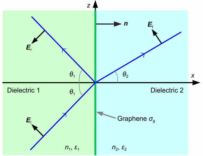
Fig. 8. Schematic model of reflection and refraction of p-polarized light passing through a dielectric-graphene-dielectric interface. The annotated parameters represent: n1 (ε1) and n2 (ε2) the refractive indices (permittivities) of dielectric 1 and 2; θ1 and θ2 the angles of incidence/reflection and refraction; E i, E r, and E t the amplitudes of incident, reflected, and transmitted electric fields; n the normal direction.
here the surface charge density of graphene ρg can be expressed using conductivity247,
Then,
Solving
From
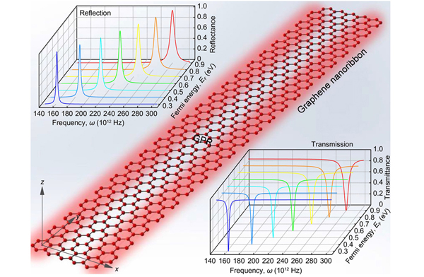
Fig. 9. Calculated dynamic transmission and reflection of light due to the GPRs in graphene nanoribbon array according to Eq. (20) . The width of graphene nanoribbon is ~100-nm-scale along x axis and infinite along y axis. The incident light is linearly polarized along x axis.
3 Metasurfaces with building blocks of structured graphene
Due to supporting the plasmon modes, naturally, graphene has been developed as the host materials for building plasmonic metasurfaces as that of noble metals, which not only extend the working frequency of metasurfaces from visible and NIR to MIR and THz but also empower the active tunability to them. To construct the GP metasurfaces, how to pattern graphene into diverse metaatoms (micro/nanostructures) is a matter of great concern. Different from bulk metals, it is difficult to structure one-atomic-thick graphene with enough degrees of freedom, leading to the poor family of metaatoms made of graphene. As discussed in Section Fundamentals of graphene, in general, there are two technology roadmaps to accomplish this task: one is directly patterning graphene into various geometric structures by advanced fabrication process39, 177, 206, 258-260, the other is spatially modulating the surface conductivity of graphene to implement equivalently patterning211, 261-264. The former usually exploits metasurfaces with functionalities of spatial EM wave manipulations in the 3D space (far-field), while the latter mainly provides the ideal platform to manipulate the surface EM wave (propagating GPs) on the 2D plane (near-field). In this Section, recent advances on dynamic spatial and surface EM wave manipulations using plasmonic metasurfaces made of structured graphene are discussed with respect to their dynamic functionalities of the spectrum modulation, wavefront shaping, polarization control, and frequency conversion in the MIR and THz regimes, which are associated with single- or multi-dimensional manipulations of the EM waves.
3.2 Dynamic spatial EM wave manipulations
3.2.1 Spectrum modulation
The localized plasmon resonances in graphene nanostructures enable the dramatic filtering of the transmission, reflection, and absorption spectra, offering an efficient way to manipulate the amplitude and frequency of light waves. External stimuli induced tunability of the resonance, such as intensity modulation and wavelength shift of the resonance, makes the spectrum modulation become active control and thereby enable dynamically tunable devices such as tunable filters, sensors, and modulators. Due to such spectral filtering in frequency domain, metasurfaces consisting of periodically patterned graphene (metaatoms) arrays are generally called frequency-selective metasurfaces, as shown in
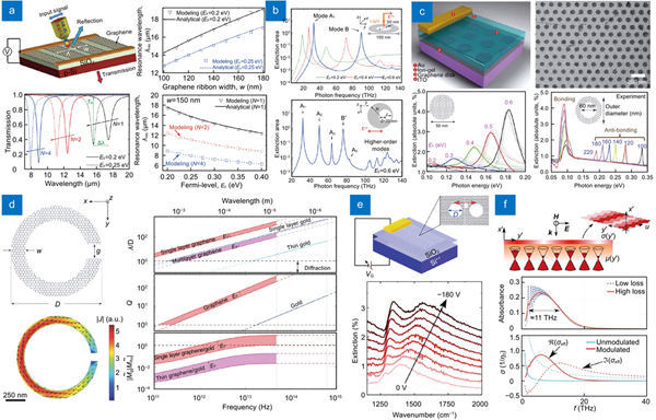
Fig. 10. Dynamic modulation of the resonance spectra using GP metasurfaces consisting of various localized plasmon resonant structures. (a ) Graphene ribbon: schematic illustration of the device, transmission spectra with different number of graphene layers, arrays with back gate, passive (with ribbon width) and active (with Fermi energy) tunings of plasmon resonance wavelength. (b ) Graphene ring: extinction area in graphene rings with symmetric and anti-symmetric structures. (c ) Graphene disk and ring: scheme of the device consisting of graphene nanodisk array, SEM image of the sample, extinction spectra of graphene nanodisks with different Fermi levels and of graphene nanorings with different outer diameters. (d ) Graphene split-ring: schematic diagram, simulated on-resonance induced current distribution, comparisons of confinement, quality factor, and the ratio of magnetic polarizability density with varying Fermi level. (e ) Graphene nanohole: schematic of the device, measured extinction spectra as a function of gate voltage. (f ) Graphene with 2D conductivity modulation: schematic of the metaatom, simulated transmission and absorption spectra. Figure reproduced with permission from: (a) ref.170, © 2013 AIP Publishing; (b) ref.265, © 2012 AIP Publishing; (c) ref.167, © 2013 ACS; (d) ref.253, Creative Commons Attribution-NonCommercial-Share Alike 3.0 Unported License; (e) ref.267, © 2018 ACS; (f) ref.268, © 2018 ACS.
The active control of the plasmon resonance spectrum is of great importance to enhance the performance of GP metasurfaces and metadevices, especially tuning and extending their working wavelength dynamically, which is very attractive for practical applications271-275. As an example, here tunable MIR plasmonic sensors using graphene metasurfaces are taken. In 2015, Rodrigo et al. reported a high-sensitivity and electrically-tunable plasmonic biosensor for detecting the protein in a label-free fashion using graphene metasurfaces272. As shown in
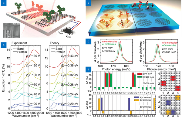
Fig. 11. Tunable biosensors of vibrational fingerprints using GP metasurfaces based on electrically-tunable spectra of GPRs. Detection of the vibrational fingerprints of proteins: (a ) conceptual view of the sensor based on electrostatically-gated graphene nanoribbon arrays, (b ) measured and calculated extinction spectra for varying bias voltage Vg and corresponding Fermi energy EF. Detection of the vibrational fingerprints and position on the sensor surface of molecules: (c ) schematic diagram of the sensor with pixeled graphene nanodisk arrays and subarrays, (d ) absorption cross-section and (e ) its variation as a function of the active pixel (position). Figure reproduced with permission from: (a, b) ref.272, © 2015 AAAS; (c–e) ref.273, © 2017 ACS.
The unit cell in the above-discussed GP metasurfaces is independent of each other, and hence the response is solely determined by the individual metaatom. However, it will be significantly different when the neighboring metaatoms are coupled. The occurrences of interesting phenomena and effects have been reported such as unprecedented levels of field enhancement by strong plasmon interaction of coupled graphene nanostructures276, 277. As its great potential in optical spectrum modulation, electromagnetically induced transparency (EIT) with the sharp and pronounced spectral response has attracted enormous attention, which has been well-studied in metallic plasmonic metasurfaces and metamaterials186. In 2013, Cheng et al. proposed a dynamically wavelength-tunable EIT metasurface in the MIR regime based on graphene nanostrips278. The metaatom consisted of the laterally coupled graphene nanostrips, i.e. one central nanostrip and two parallel nanostrips, as shown in
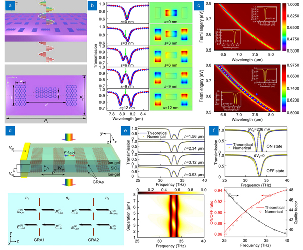
Fig. 12. Coupling-induced dynamic spectrum modulation with the tunable EIT features using GP metasurfaces. Near-field-coupled graphene nanostrips: (a ) schematic model, (b ) transmission spectra and plasmon mode distribution with varying coupling distances, (c ) transmission spectra as a function of Fermi energy for coupling distances of s=0 and 12 nm. Phase-coupled graphene ribbons: (d ) schematic configuration and transfer matrix model, (e ) transmission dependence on different separations h, (f ) demonstration of electro-optical switch based on the graphene metasurface. Figure reproduced with permission from: (a–c) ref.278, © 2013 AIP Publishing; (d–f) ref.248, © 2014 AIP Publishing.
3.2.2 Wavefront shaping
Besides the amplitude manipulation, plasmon resonances in graphene nanostructures can also effectively produce the scattering phase retardation, which is strongly associated with the geometry and wavelength. Recently, GP metasurfaces have been widely demonstrated to control the wavefront of light based on the amplitude and phase manipulations. Here, we will discuss the research progress on graphene-based dynamic metasurfaces for active wavefront shaping. To start with, the phase and amplitude manipulation by graphene nanoribbon metasurfaces are shown in
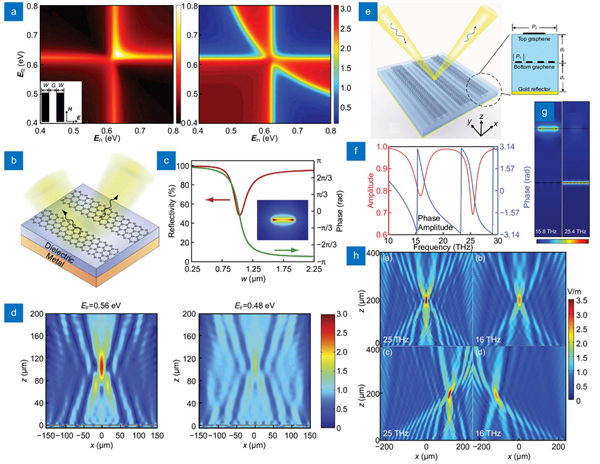
Fig. 13. Dynamic wavefront shaping using GP metasurfaces based on resonance phase. (a ) Scattering amplitude and phase as the function of Fermi level of the unit cell with two graphene nanoribbon. FP cavity-enhanced graphene metasurface: (b ) schematic of metasurfaces, (c ) reflectivity and phase of the reflected light as a function of ribbon width, (d ) focusing performance at different Fermi levels. Dual-band light focusing reflector using stacked graphene nanoribbon metasurfaces: (e ) schematic model, (f ) amplitude and phase responses of the reflected light, (g ) the relative electric field distributions at resonant frequencies of 15.8 and 25.4 THz, (h ) simulated performances of the dual-band focusing reflector. Figure reproduced with permission from: (a) ref.285, © 2014 John Wiley and Sons; (b–d) ref.286, Creative Commons Attribution 4.0 International License; (e–h) ref.288, © 2017 ACS.
As above discussions, by tailoring the structural parameters of a single graphene antenna such as ribbon, the abrupt phase modulation of π arising from the plasmon resonance can be introduced. To extend the phase modulation to cover the entire 2π range, multiple independent resonances and coupled antenna resonances have been developed. In addition, the Pancharatnam-Berry (PB) phase based on the orientations of antennas is another efficient method, in fact a completely different one, to implement 2π phase modulation. The PB phase, or geometric phase, is associated with the space-variant conversion of polarization states following the path on the Poincaré sphere, which can be created by anisotropic subwavelength antennas with identical geometric parameters but spatially varying orientations291. The phase difference between the transmitted/reflected waves from any two points on the metasurface equals to one-half of the solid angle enclosed by their corresponding traces on the Poincaré sphere292. For the CP incident wave, the handedness of transmitted/reflected CP wave is opposite with an additional PB phase of twice the rotation angle of antenna, which means that the entire 2π phase range can be covered by only rotating antenna from 0 to 180º in metasurfaces. Currently, the PB phase has been widely developed to completely shape the wavefront of CP waves using plasmonic and dielectric metasurfaces4, 13, 31, 46. Based on such PB phase principle, graphene metasurfaces have also been demonstrated to dynamically control the wavefront of CP light. In 2015, Cheng et al. proposed a graphene metasurface with periodically patterned graphene nanocrosses (as illustrated in
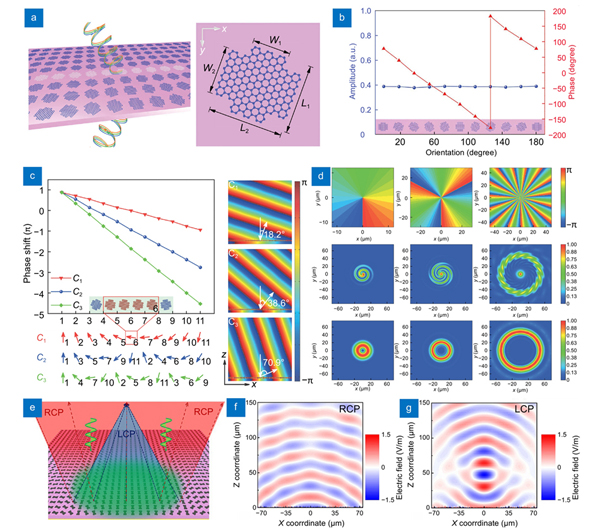
Fig. 14. Dynamic wavefront shaping using GP metasurfaces based on PB phase. Transmission-type graphene nanocrosses metasurface: (a ) schematic model, (b ) transmission amplitude and phase profiles of the CP light at the frequency of 17 THz. Reflection-type graphene nanocrosses metasurface: (c ) reflective phase shifts and simulated phase distributions of three different arrangements (C1, C2, and C3), (d ) phase distributions, interferograms, and far-field electric distributions for 1-order, 3-order, and 15-order vortex-beam-generating metasurfaces. The spin-dependent flat lens: (e ) schematic of the flat lens metasurface, (f ) electric field map under RCP incidence, (g ) electric field map under LCP incidence. Figure reproduced with permission from: (a, b) ref.77, © 2015 John Wiley and Sons; (c, d) ref.122, © 2018 John Wiley and Sons; (e–g) ref.293, © 2019 OSA, under the terms of the OSA Open Access Publishing Agreement.
3.2.3 Polarization control
To control the polarization state of light, the Faraday effect is a universal train of thought. In the magnetic field, Faraday rotation of several degrees in the continuous graphene has been demonstrated experimentally by Crassee et al. in 2011294. Unfortunately, such giant rotation of the polarization state is typically at lower THz frequency due to the intrinsic cyclotron resonance of massless carriers and meanwhile requires giant magnetic fields, which hinder their applications. To extend the operation range and enhance the maximum rotation angle in smaller magnetic fields, creating metasurfaces with structured graphene to break the uniformity of a continuous graphene sheet has been demonstrated as an efficient way295. By patterning graphene into microribbon array, as shown in
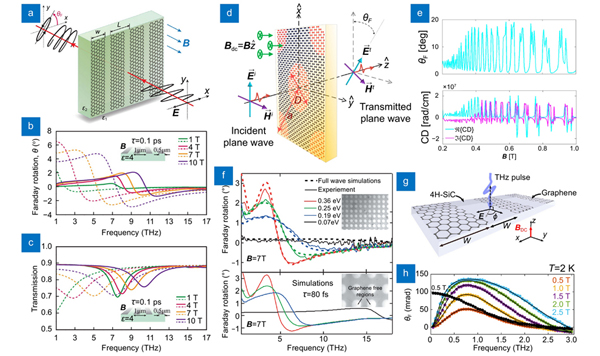
Fig. 15. Dynamic polarization rotation in graphene metasurfaces based on the magnetoplasmon-enhanced Faraday effects. Graphene microribbon array: (a ) schematic Faraday rotation, (b ) Faraday rotation and (c ) transmission spectra of ribbon arrays and continuous graphene on top of the substrate (ε=4) with relaxation time τ=0.1 ps at various magnetic fields. Equivalent graphene nanodisk array (by spatially modulating conductivity): (d ) schematic far-field Faraday rotation, (e ) Faraday rotation angle and (f ) circular dichroism versus magnetic field at the frequency of 42.7 THz. (f) Measured and simulated Faraday rotation spectra of graphene square antidot (GSA) array at different magnetic fields (the inset: SEM pictures of GSA). (g ) Schematic model and (h ) Faraday rotation spectrum of the graphene micro-ribbon metasurface for normally incident THz pulses at different external magnetic fields. Figure reproduced with permission from: (a–c) ref.296, © 2013 ACS; (d, e) ref.297, © 2014 ACS; (f) ref.298, © 2018 APS; (g, h) ref.299, © 2020 AIP Publishing.
Apart from the Faraday effect, polarization-dependence of the plasmon resonances in structured graphene has already been exploited to implement dynamic polarization control. Due to the geometric symmetry, plasmon resonances in graphene disk and ring are polarization-independent. While for asymmetric graphene structures such as ribbon, rectangle, ellipse, and cross the plasmon resonances are highly sensitive to the polarization state of incident light. In 2013, Cheng et al. proposed a MIR tunable polarization converter by using asymmetric graphene nanocrosses300. As shown in
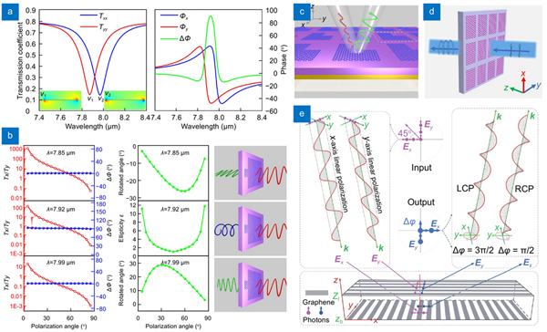
Fig. 16. Dynamic polarization conversion in GP metasurfaces based on polarization-dependent plasmon resonances. Asymmetric graphene nanocrosses metasurfaces: (a ) transmission coefficients and phase difference excited by linearly polarized light, (b ) transmission amplitude ratio, phase difference, rotated polarization angle, and ellipticity versus the incident polarization angle at three wavelengths. (c ) L-shaped graphene nanostructures. (d ) Rectangular graphene patches. (e ) The operation principle of the polarization converter based on crossed-graphene ribbon gratings. Figure reproduced with permission from: (a, b) ref.300, © 2013 OSA, under the terms of the OSA Open Access Publishing Agreement; (c) ref.301, © 2013 AIP Publishing; (d) ref.302, © 2016 OSA; (e) ref.304, © 2018 OSA, under the terms of the OSA Open Access Publishing Agreement.
3.2.4 Frequency conversion
On the way to seek nonlinear materials with low threshold and ultrafast response time, plasmonic nanostructures have been particularly attractive because of their ability to enhance the electric field intensity near nanostructures, such as noble metal nanoparticles and metasurfaces. Although the third-order nonlinear effects including four-wave mixing (FWM), Kerr effect, and third-harmonic generation have been experimentally confirmed in the undoped graphene, even-order nonlinear processes are always forbidden because graphene is a centrosymmetric atomic crystal. To exploit the even-order nonlinearity, Cox and García de Abajo demonstrated theoretically that graphene nanoislands could be an ideal platform for developing the electrically-tunable nonlinear nanodevices305. As shown in
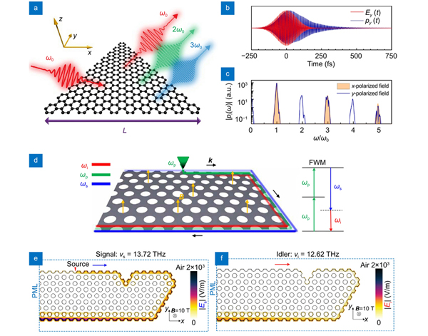
Fig. 17. Dynamic nonlinear frequency conversion using GP metasurfaces. Harmonic generation in the armchair-edged triangular graphene nanoislands: (a ) illustration of nanoisland and harmonic generation, (b ) time-varying graphene dipole induced by the electric field of incident pulse, (c ) excitation of harmonics for incident pulses with polarizations along the x and y directions. Topologically protected FWM interactions in a specific graphene metasurface: (d ) configuration of a periodic nanohole array in a graphene sheet and FWM of topologically protected one-way edge plasmons, near-field profiles at the frequencies of signal (e ) and idler (f ). Figure reproduced with permission from: (a–c) ref.305, © 2014 Springer Nature; (d–f) ref.127, © 2020 The authors, under a Creative Commons Attribution License 4.0 (CC BY).
3.3 Dynamic surface EM wave manipulations
As discussed in Section Theoretical and numerical models of GPs, graphene shows good energy confinement and guidance of propagating GPs, and has been demonstrated as a one-atom-thick platform for 2D nanophotonic waveguides in the MIR and THz frequencies. Furthermore, the spatial conductivity patterning method proposed by Vakil and Engheta provides an efficient way to actively guide and manipulate the GPs propagating along with graphene sheet, which has attracted increasing attention of researchers in the nanophotonics community310. In fact, this method was initially adopted to create functional GP-waveguide devices by implementing special gate-voltage scheme or directly patterning the Fermi energy of graphene. For example, GP-waveguide switches at NIR frequency were achieved by selectively enabling or forbidding propagation of GPs311; THz GP-waveguide array was proposed with negligible crosstalk by patterning the ferroelectrics into parallel- and antiparallel-poling configurations, which can induce drastically different carrier densities at the different domain of graphene sheet221; Nanofocusing of propagating GPs on graphene sheet in the MIR band was realized by using spatially gradient chemical potential220.
For more complex manipulation of propagating GPs on graphene, the metasurface concept has been introduced into the 2D GP-waveguide system. According to the spatial conductivity patterning method, the capacitor model is the fact of the matter. By using a silicon-based grating structure as the ground plate of the graphene-silica-silicon capacitor, as shown in
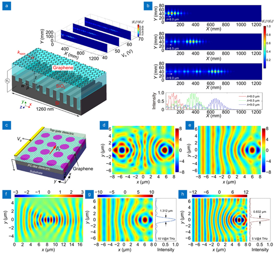
Fig. 18. Dynamic trapping and focusing of GP waves propagating along the 2D plane of graphene sheet using GP metasurfaces. GP metasurface with a groove grating silicon as the ground plate of the parallel capacitor: (a ) schematic model with a graded grating silicon plate, (b ) electric fields of GP waves for different wavelengths. GP metasurface with PC-like dielectric layer underneath graphene sheet: (c ) fundamental structure model, field distributions of Maxwell’s Fisheye lens (d ), Luneburg lens (e ), self-focusing lens (f ), and Luneburg lens at different gate voltages (g ) and (h ). Figure reproduced with permission from: (a, b) ref.312, 2015, (c–h) ref.263, 2014, under a Creative Commons Attribution 4.0 International License.
Based on the similar method, in 2019, Basov et al. experimentally demonstrated a broadly tunable 2D PC platform for on-chip plasmonic manipulation using graphene metasurface, which consisted of a hBN encapsulated single-layer graphene on top of a hexagonal lattice array of SiO2 pillars, as shown in
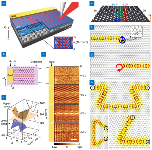
Fig. 19. Dynamic guiding of GP waves propagating along the 2D plane of graphene sheet using GP metasurfaces. GP metasurface with patterned substrate underneath a fully encapsulated graphene sheet: (a ) schematic configuration, (b ) schematic metasurface with an engineered domain wall, (c ) calculated plasmonic band structure, (d ) experimental near-field images at different gate voltages. GP metasurface with periodically patterned air nanoholes in a graphene sheet: (e ) schematic of GP metasurface waveguide by mirror-symmetrically putting two optimized GP metasurfaces together, unidirectional mode propagations of RCP (f ) and LCP light (g ), backscattering-immune propagations in U-, C-, and L-bend domain-wall interfaces (h ). Figure reproduced with permission from: (a–d) ref.314, 2019, under a Creative Commons Attribution 4.0 International License; (e–h) ref.315, © 2020 IEEE.
4 Hybrid metasurfaces integrated with graphene
Although the manipulations of amplitude, phase, and polarization of EM waves have been well studied using metallic and dielectric metasurfaces, such manipulations are usually passive with the before-fabrication variation of the size, shape, and material properties of the metaatoms and metasurfaces. Beyond patterning graphene into plasmonic nanostructures as aforementioned discussions, integrating graphene with passive metasurfaces is another mainstream route to enable dynamically tunable functionalities due to the fairly mature fabrication processes and larger degrees of freedom for 3D bulky materials (such as metals and dielectrics) when compared with 2D materials (such as graphene). As discussed in Section Basic material properties of graphene, the surface conductivity (or dielectric function, or surface resistance) of graphene is electrically tunable with great ease via an external electric field, which is rather attractive for empowering activity to passive metasurfaces and metadevices. In general, the dynamic tunability of a conventional passive metasurface can be actualized by putting an electrically-controlled graphene layer in its proximity, which significantly influences the EM response of the metasurface usually ultra-sensitive to the surrounding environment where graphene locates. In 2012, Min et al. experimentally demonstrated a gate-controlled graphene-integrated metasurface to dynamically modulate both the amplitude and phase of THz wave, and due to the strong coupling of graphene with metaatoms the measured maximum values of amplitude and phase changes exceeded 47% and 32.2° respectively74. At the same time, Boltasseva et al. experimentally demonstrated the electrical control of the plasmonic resonances in an infrared regime by fabricating metal nanostructures on a voltage-controlled graphene layer, which largely enhanced the light-graphene interaction and in turn strongly impacted the damping of plasmonic resonances316. In 2013, Capasso et al. demonstrated the electrical tuning of plasmonic resonances using graphene-loaded antennas over a broad wavelength range of 650 nm at the MIR frequencies317. In 2015, Khanikaev et al. introduced a theoretical model for enhancing the nonlinear response of graphene through graphene-integrated plasmonic metasurfaces, which numerically proved the tunable nonlinear frequency conversion318. Inspired by those works, the combination of graphene and metallic structures including metasurfaces emerges as a wonderful platform for exploiting electrically-controlled nanodevices319-327. Tremendous attention have been paid to the graphene-hybrid metasurfaces for dynamically EM wave manipulating328-330. For such hybrid metasurfaces, their manipulations of amplitude, phase, and/or polarization of EM waves mainly depend on metasurfaces and graphene in general propels such manipulations from static to dynamic. In this Section, graphene-hybrid metasurfaces are distinguished with respect to their control manners with graphene including the global and local ways. Several typical examples on homogeneous metasurfaces and digital coding metasurfaces are discussed in detail based on globally- and locally-controlled graphene, respectively.
4.2 Homogeneous metasurfaces based on globally-controlled graphene
Homogeneous metasurface refers to the metasurface in which its metaatoms are simultaneously controlled by one graphene layer, which results in the global-controlled response of all metaatoms when gate voltage is applied. Here, dynamic spectrum modulations related to amplitude change and frequency shift are presented first. To explore a high-speed and high-contrast amplitude modulator, Yao et al. proposed an electrically-tunable MIR perfect absorber by incorporating a graphene-integrated metasurface into a subwavelength-thick optical cavity, as shown in
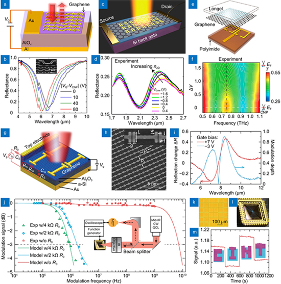
Fig. 20. Dynamic spectrum modulations using graphene-hybrid metasurfaces. Ultrathin MIR amplitude modulators based on electrically tunable metasurface perfect absorber: (a ) schematic of metasurface modulator comprising plasmonic structures on graphene, (b ) measured reflection spectra for different gate voltages (inset: SEM image of the metasurface on graphene). Electrical modulation of Fano resonance in plasmonic metasurface using graphene: (c ) schematic illustration of the Fano resonant metasurface fabricated on top of graphene with Si back gate, (d ) measured reflectance spectra of the metasurface with ion-gel top electrolyte at different gate voltages. Electrically tunable EIT and slow light using diatomic metasurface integrated with a gated graphene: (e ) schematic view of gate-controlled EIT metasurface, (f ) measured transmission spectra as a function of gate voltage variation. Hybrid graphene metasurfaces for SLM: (g ) schematic of the metasurface, (h ) SEM image, (i ) reflection change and modulation depth as functions of wavelength at gate biases of 7 V (red curve) and -3 V (blue curve), (j ) modulation speed (inset: measurement system) of the SLM, (k ) optical micrograph of 6×6 functional pixels, (l ) photograph of the device, (m ) spatial reflection patterns of “CINT” by selectively applying gate voltages to individual pixels. Figure reproduced with permission from: (a, b) ref.75, © 2014 ACS; (c, d) ref.332, © 2014 ACS; (e, f) ref.335, © 2018 ACS; (g–m) ref.337, under a Creative Commons Attribution 4.0 International License.
For the phase manipulations, in fact, the aforementioned amplitude manipulations are at the same time accompanied by the phase manipulation due to the electric or magnetic resonances in metasurfaces. This resonance-induced phase retardation has been widely employed to realize dynamic phase modulation of EM waves by a variety of gate-controlled graphene metasurfaces. For instance, Zhou et al. proposed a gate-graphene magnetic resonant metasurface to achieve widely tunable phase modulation of reflected THz waves, where graphene was utilized as a tunable loss to drive the coupling behavior in metasurface338; Shvets et al. demonstrated the 55° phase control of the reflected MIR light while maintaining the amplitude constant using a plasmonic metasurface integrated with a graphene sheet339; Atwater et al. reported up to 237° phase modulation range using electronically reconfigurable graphene-gold resonator metasurfaces340. Besides the above-discussed resonance phase, the PB phase has been extensively investigated to conceive metallic and dielectric metasurfaces for phase manipulation due to its advantages of broadband operation, easy access and large tolerance of design29, 46, 341, 342. Recently, integrating graphene with those metasurfaces based on PB phase renders the phase manipulation more active, enabling the dynamic wavefront control. In 2017, Zhang et al. demonstrated the graphene-integrated metasurfaces and metalens based on PB phase for actively modulating the electric-field amplitude (or intensity) of anomalously refracted THz waves343. The demonstrated active metasurface consisted of a graphene sheet deposited on the array of U-shaped apertures, as shown in
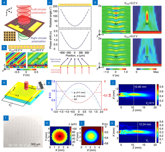
Fig. 21. Dynamic wavefront control using graphene-hybrid metasurfaces. Electrically modulation of anomalously refracted THz waves with gated-graphene metasurfaces: (a ) schematic view of the crosspolarized transmission in graphene metasurfaces consisting of a graphene sheet deposited on the array of U-shaped apertures (inset: optical micrograph image), (b ) schematic of the metasurface with linear phase variation and the simulated wavefront control for LCP incidence at different gate voltages, (c ) metasurface with parabolic phase profile for focusing THz waves, (d ) electrically modulations of electric field and energy density of focusing performances. Graphene-enabled electrically controlled THz metalens: (e ) schematic of the active THz metalens composed of an Au metasurface and a graphene layer, (f ) SEM micrograph of the fabricated metalens, (g ) phase distributions of metalens with focal lengths of 7 mm and 9 mm and their phase difference, (h ) length L and (i ) rotation angle θ distributions of the metalens, (j ) and (k ) far-field intensity distributions of the transmitted RCP THz waves at gate voltages of 0 and 2 V respectively. Figure reproduced with permission from: (a–d) ref.343, © 2017 Wiley; (e–k) ref.344, © 2018 Chinese Laser Press.
Similar to the aforementioned dynamic amplitude and phase manipulations, dynamic manipulation of the polarization state using graphene-hybrid metasurfaces has attracted enormous interest. To manipulate the polarization state, the anisotropy of metasurfaces plays a dominant role, in which the different responses along orthogonal principal axes of the metaatoms lead to different amplitude attenuation and phase retardation of the incident EM waves345-347. Therefore, the polarization state can be controlled with great ease through carefully engineering the geometries of metaatoms, and further dynamic control of the polarization state can be realized by integrating gate-graphene with metasurfaces, where graphene is often deposed in hot spots created by metasurface to actively adjust the anisotropic responses of metasurfaces, i.e. tuning the amplitude attenuation and phase retardation. On the basis of this principle, Tian et al. proposed a metadevice by integrating graphene with an anisotropic metasurface, as shown in
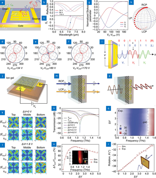
Fig. 22. Dynamic polarization control using graphene-hybrid metasurfaces. Mid-infrared optical polarization encoding using graphene-integrated plasmonic metasurfaces: (a ) schematic illustration of the polarization encoding process based on the circular orthogonal polarization basis, (b ) and (c ) reflection and normalized Stokes parameter S3 spectra at different gate voltages as functions of wavelength, (d -f ) polarization states of the reflected light under linearly polarized incident light at three different gate voltages, (g ) normalized Stokes parameters (S1, S2, S3) as a function of gate voltage, (h ) corresponding polarization states on the Poincaré sphere, (i ) schematic illustration of the PDM technique realized by the proposed metadevice. Electrical tuning of the polarization state of THz waves using graphene chiral metasurfaces: (j ) schematic rendering of the conjugated double Z metasurface with the ion-gel gate, (k ) and (l ) electric field distributions for RCP and LCP in the metasurfaces at the frequency of 1.1 THz at gate voltages of 0 and 1.8 V respectively, (m ) schematic of CD transmission, (n ) measured transmission spectra for RCP and LCP waves at different gate voltages, (o ) measured and simulated intensity modulation depth as a function of gate voltage (inset: measured CD with different gate voltages), (p ) schematic of OA transmission, (q ) measured ellipticity with different gate voltages, (r ) azimuthal rotation angle θ at the frequency where η=0 as a function of gate voltage. Figure reproduced with permission from: (a–i) ref.348, © 2016 John Wiley and Sons; (j–r) ref.349, under a Creative Commons Attribution NonCommercial License 4.0 (CC BY-NC).
4.3 Digital coding metasurfaces based on locally-controlled graphene
Compared with homogeneous metasurfaces based on globally-controlled graphene, it is highly desired to independently control the unit cells of metasurfaces, which provides more degrees of freedom and possibilities for manipulating EM waves. In order to explore the distinct abilities for manipulating EM waves in programmable manners, in 2014, Cui et al. proposed a new concept of digital metamaterials, which has advanced metamaterials and metasurfaces more controllable, multi-functional, and intelligent350-352. In general, the core feature of digital metamaterials relies on the independently-controllable metaatom or array of several metaatoms. In 2018, Balci et al. demonstrated an electrically reconfigurable digital metadevice working in microwave frequencies with the assistance of locally-controlled graphene79. Firstly, the electrical control of both amplitude and phase of microwave was theoretically and experimentally investigated in graphene-integrated split-ring resonator (SRR) metasurfaces. Then, based on the digital metasurface concept, they proposed a digital metadevice with spatially varying dielectric constant to implement voltage-controlled adaptive transformation optics. As shown in
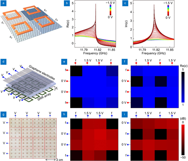
Fig. 23. Electrically reconfigurable digital graphene-hybrid metadevices with spatially varying dielectric constant. (a ) Schematic of a digital metasurface with individually addressable pixels, (b ) and (c ) calculated real and imaginary part of the effective dielectric constant in a single pixel as functions of bias voltages, (d ) schematic of the pixelated metadevice, (e ) and (f ) spatial maps of the real part of the dielectric constant at different voltage configuration, (g ) photograph of fabricated metadevice with 4×4 arrays of active pixel containing 3×3 SRRs, (h ) and (i ) measured transmission patterns corresponding to (e) and (f) respectively. Figure reproduced with permission from ref.79, under a Creative Commons Attribution NonCommercial License 4.0 (CC BY-NC).
More recently, a programmable graphene-metal hybrid metasurface for dynamic wavefront control of the microwave was experimentally reported by Chen et al., based on which dynamic functions including beam redirecting and Radar cross section (RCS) reduction was achieved with binary phase coding353. As shown in
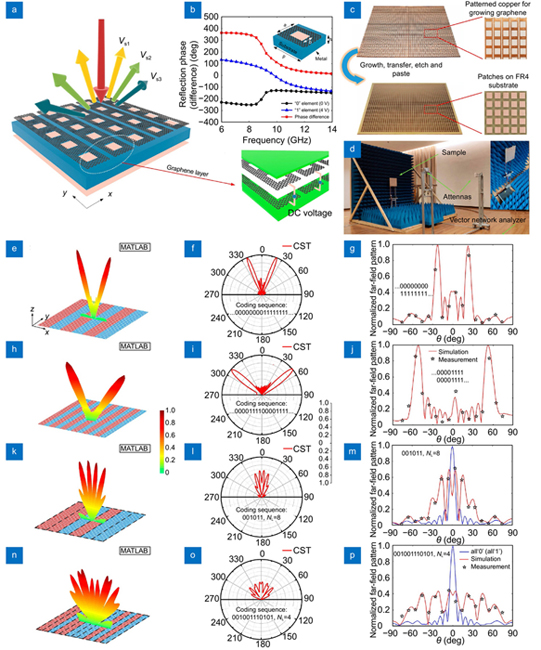
Fig. 24. Programmable graphene-hybrid metasurfaces for dynamic wavefront control. (a ) Conceptual illustration of the metasurface, (b ) phase of the reflected waves from the coding graphene metasurface elements, (c ) photograph of fabricated metasurfaces, (d ) measurement system, (e -g ) calculated, simulated, and measured far-field results for beam redirecting at the coding sequence of...0000000011111111..., (h -j ) results for beam redirecting at the coding sequence of...0000111100001111..., (k -m ) results for RCS reduction at the coding sequence of 001011 with 8 unit cells in a lattice, (n -p ) results for RCS reduction at the coding sequence of 001001110101 with 4 unit cells in a lattice. Figure reproduced with permission from ref.353, © 2020 ACS.
Actually, complete manipulation of EM waves requires the arbitrary control of both phase and amplitude. However, most of the digital coding metasurfaces solely depend on the phase shift while the amplitude response is usually fixed. To address this issue, Zhang et al. directly introduced the independent amplitude modulation into phase coding metasurface by designing a graphene-based digital coding metasurface for dynamical and continuous wavefront control of reflected wave in the microwave band354. This metasurface was mainly composed of metallic structures and a graphene sandwich structure with fishnet patterns, as shown in
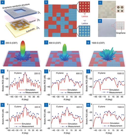
Fig. 25. Dynamic scattering steering using graphene-integrated digital coding metasurfaces. (a ) 3D schematic of the metaatom consisting of five layers: graphene layer, spacer, metal pattern, substrate, and ground layer, (b ) optimal coding distributions of the proposed metasurface, (c ) and (d ) photograph of metal patterned layer and graphene patterned layer, (e -g ) simulated 3D scattering patterns at different surface resistances of graphene, (h -m ) measured bistatic RCS of the proposed coding metasurface in the H- and E-plane. Figure reproduced with permission from ref.354, © 2020 John Wiley and Sons.
5 Conclusion and outlook
To summarize, we have provided a comprehensive review of the dynamic metasurfaces and metadevices enabled by graphene, including metasurfaces with building blocks of structured graphene and metasurfaces hybridly-integrated with graphene, with our focus on electrically-controlled dynamical manipulation of the EM waves covering the MIR, THz, and microwave regimes. Before discussing the state-of-the-art developments, the fundamentals of graphene as diverse as the basic material properties, plasmons in graphene, and in particular the theoretical and numerical models of GPs are described in details. Above all, the dynamic functionalities of the spectrum manipulation, wavefront shaping, polarization control, and frequency conversion in both near/far fields and global/local manners are elaborated using graphene-empowered metasurfaces and metadevices. As a comparative comment, it should be emphasized that the ultrabroadband and continuous tunability of graphene by external electrical stimuli empowers the metasurfaces and metadevices with the real-time, dynamical tunability over almost the entire spectrum of EM waves, which can never be accomplished currently by other solutions such as phase-change materials and transparent conducting oxides. Although chip-integrated MIR metadevices and microwave programmable metadevices using graphene have been already reported, it does not mean that graphene metasurfaces have been developed sufficiently. Here, we would like to underline that the investigation is just started in terms of the emerging concept in dynamic metasurfaces and widely potential applications in the future. Currently, this field is experiencing the explosive developments, where opportunities and challenges coexist.
For metasurfaces based structured graphene, their developments highly depend on the design method and nanofabrication techniques for graphene patterns in particular with more complicated geometry and larger footprint. For the design methods, as the demands of performance and functionality growing, the pattern design and optimization of metasurfaces and metadevices become computationally expensive and time-inefficient. To overcome such challenge, the artificial intelligence-based algorithms for smart inverse design show great potentials, which can search the parameter space in a more efficient way, leading to the on-demand design of novel metasurfaces and metadevices with tremendous complexity355, 356. For the nanofabrication techniques, currently, the simple and periodic graphene patterns such as ribbons, disks, and rings are widely fabricated by using standard electron-beam lithography (EBL) followed by plasma etching. To achieve polarization and/or phase manipulations, however, the anisotropic and aperiodic graphene patterns are indispensable, which requires high-quality nanofabrication technique because the defect and edge effects of graphene patterns strongly impact the polarization and phase responses of EM waves. For example, to efficiently exploit the PB phase for dynamic wavefront shaping, it is essential to arrange the anisotropic graphene patterns with varying rotation angles, which have not yet been experimentally validated due to the fabrication challenge for high-quality graphene patterns. Besides the EBL, recently-developed direct laser writing technique may provide a promising alternative to address this challenge by right of the advantages of mask-free and resist-free, which can avoid degenerating the quality of graphene patterns induced by the complex procedures in EBL and simultaneously enhance the fabrication efficiency for complex patterns114, 357, 358. Before the pattern fabrication, the challenges to achieve consistent, large-scale, transfer-free, and layer-number-controlled graphene films are worth mentioning, which to some extent determines the viability of the fabrication technology. To address these challenges, the graphene oxide routine has been recently demonstrated as a new solution by Jia et al., where the solution-phase preparation of the high-quality and large-scale graphene oxide layer is firstly performed, and then controllable conversion from graphene oxide layer into graphene layer is accomplished based on laser photoreduction359. Moreover, such laser patterning technique naturally results in equivalent fabrication of functional photonic devices for integrated photonics and flat optics360. To date, they have experimentally reported an ultrabroadband graphene oxide flat lens for wavefront shaping and an ultrathin graphene metamaterial for extremely broadband absorption of unpolarized light260, 361. This low-cost and scalable method provides unprecedented control over the layer thickness, number, and pattern in particularly designing and fabricating multilayer graphene-based metamaterials, which exhibit great potentials in the future. In addition, the new metasurface concept, such as on-chip metasurfaces and time-variant metasurfaces50, 362-365, and functionalities as that of metallic and dielectric counterparts are highly expected to be transplanted into graphene-based metasurfaces and metadevices such as multidimensional EM wave manipulations.
For graphene-hybrid metasurfaces, the future in fact goes along with the development of conventional passive metasurfaces including concept and fabrication. A number of experimental works have proved that integrating graphene layer to the metallic or dielectric metasurfaces and metadevices can transform the passive metadevices to be more active and multifunctional, which are extremely desired for integrated photonic applications. Despite the rapidly growing demand, dynamic metasurfaces lag behind passive metasurfaces in terms of the functionalities. The dynamic versions of many intriguing functionalities have not been actualized experimentally using graphene-hybrid metasurfaces, including dynamic holography, encryption, orbital-angular momentum multiplexing and demultiplexing, etc. The challenges mainly exist in integrating high-quality graphene layer to metasurfaces and metadevices, and also fabricating the electrodes without influence on the quality of graphene. Generally, the dynamic tunability of a metasurface is actualized by putting a graphene layer in its proximity, which significantly influences the EM response of the metasurface. Such dynamic tuning is widely implemented by electrical method using metallic electrode or graphene electrode, which challenge the fabrication process and also limit the tuning speed as well as footprint of metadevices. To overcome the speed limitation of electric switches, all-optical control is a promising direction based on the optical nonlinearity of graphene enhanced by the extreme light confinement in metasurface, which can also greatly reduce the device footprint without electrodes366. The dynamic manipulations of amplitude, phase, and polarization have been reported in the NIR, MIR, and THz regimes by globally-controlled graphene-hybrid metasurfaces and in the microwave band by locally-controlled graphene-hybrid metasurfaces. However, due to the difficulty of locally controlling the individual metaatoms in metasurfaces at the shortwave frequencies, where the sizes of metaatoms and metasurfaces are smaller than that at the longwave frequencies, manipulating the EM waves in the NIR, MIR, and THz regimes by programmable manners based on the digital metasurface concept remains challenges.
At last, dynamic metasurfaces and metadevices enabled by other graphene-like 2D materials, such as BP, TIs, and TMDCs, are also an attractive direction367-373. Besides electrical tunability, 2D materials beyond graphene can empower more unique advantages to metasurfaces and metadevices, such as nonlinearity together with optical controllability, which will undoubtedly expand the degrees of freedom in EM wave manipulation and improve the modulation speed by optical-controllable metasurfaces. Several research groups have recently focused on the 2D materials-based metasurfaces to explore the new value of 2D materials and metasurfaces. For example, Novotny et al. demonstrated controllable steering of the second harmonic (SH) emission by coupling a monolayer MoS2 onto an optical phased array consisting of gold antennas374; By integrated WS2 with Au plasmonic nanosieve metasurfaces, Lu et al. reported the SH metalens, OAM generation, beam steering, polarization control, and holograms375-377; Zentgraf et al. proposed a WS2-integrated plasmonic metasurface based on PB phase to modulate the polarization and phase of SH signal378. Those pioneering works offer new opportunities for dynamically generating and manipulating the EM waves by nonlinear means. With the all potential future directions and gradually improved nanofabrication technique, we believe that the dynamic metasurfaces and metadevices using graphene and further graphene-like 2D materials will certainly revolutionize the EM wave manipulations and finally commercialized applications in the future.
[10] Kamali SM, Arbabi E, Arbabi A, Horie Y, Faraji-Dana M et alAngle-multiplexed metasurfaces: encoding independent wavefronts in a single metasurface under different illumination anglesPhys Rev X20177041056
[14] Guo JY, Wang T, Quan BG, Zhao H, Gu CZ et alPolarization multiplexing for double images displayOpto-Electron Adv20192180029
[47] Ma XL, Pu MB, Li X, Guo YH, Luo XGAll-metallic wide-angle metasurfaces for multifunctional polarization manipulationOpto-Electron Adv20192180023
[49] Yu NF, Capasso FFlat optics with designer metasurfacesNat Mater20141313915010.1038/nmat3839
[52] Sain B, Meier C, Zentgraf TNonlinear optics in all-dielectric nanoantennas and metasurfaces: a reviewAdv Photonics20191024002
[66] Cala Lesinà A, Goodwill D, Bernier E, Ramunno L, Berini PTunable plasmonic metasurfaces for optical phased arraysIEEE J Sel Top Quantum Electron2021274700116
[73] Shen ZX, Zhou SH, Li XN, Ge SJ, Chen P et alLiquid crystal integrated metalens with tunable chromatic aberrationAdv Photonics20202036002
[93] Nemati A, Wang Q, Hong MN, Teng JHTunable and reconfigurable metasurfaces and metadevicesOpto-Electron Adv20181180009
[100] He Q, Sun SL, Zhou LTunable/reconfigurable metasurfaces: physics and applicationsResearch201920191849272
[130] Geim AK, Novoselov KSThe rise of grapheneNat Mater2007618319110.1038/nmat1849
[168] Wang GX, Liu XM, Lu H, Zeng CGraphene plasmonic lens for manipulating energy flowSci Rep201444073
[192] Luo XGPlasmonic metalens for nanofabricationNatl Sci Rev2018513713810.1093/nsr/nwx135
[226] Balanis CA. Advanced Engineering Electromagnetics 2nd ed (John Wiley & Sons, Inc., New York, 2012).
[241] Song JCWPlasmon propagation pushed to the limitNature201855750150210.1038/d41586-018-05190-1
[258] Xiong W, Zhou YS, Hou WJ, Jiang LJ, Gao Y et alDirect writing of graphene patterns on insulating substrates under ambient conditionsSci Rep201444892
[262] Vakil A, Engheta NFourier optics on graphenePhys Rev B20128507543410.1103/PhysRevB.85.075434
[338] Miao ZQ, Wu Q, Li X, He Q, Ding K et alWidely tunable terahertz phase modulation with gate-controlled graphene metasurfacesPhys Rev X20155041027
[368] Arezoomandan S, Gopalan P, Tian K, Chanana A, Nahata A et alTunable terahertz metamaterials employing layered 2-D materials beyond grapheneIEEE J Sel Top Quantum Electron2017238500307
[377] Hong XM, Hu GW, Zhao WC, Wang K, Sun S et alStructuring nonlinear wavefront emitted from monolayer transition-metal dichalcogenidesResearch202020209085782
Article Outline
Chao Zeng, Hua Lu, Dong Mao, Yueqing Du, He Hua, Wei Zhao, Jianlin Zhao. Graphene-empowered dynamic metasurfaces and metadevices[J]. Opto-Electronic Advances, 2022, 5(4): 200098.
