Author Affiliations
Abstract
1 Photonics Information Innovation Center and Hebei Provincial Center for Optical Sensing Innovations, College of Physics Science & Technology, Hebei University, Baoding 071002, China
2 State Key Laboratory of Optoelectronic Materials and Technologies, School of Electronics and Information Technology, Sun Yat-sen University, Guangzhou 510275, China
3 e-mail: caixlun5@mail.sysu.edu.cn
4 e-mail: syao@ieee.org
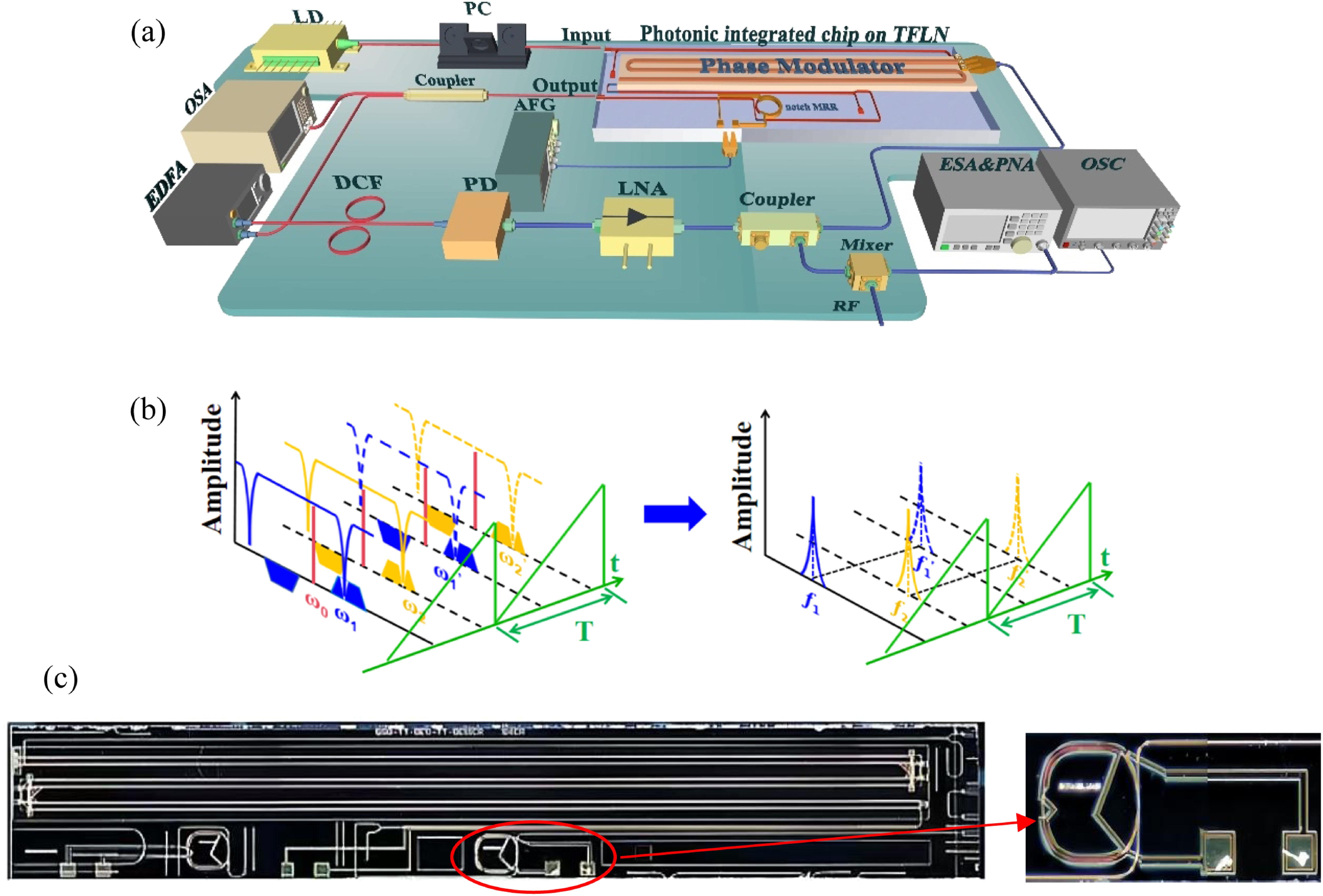
Linearly chirped microwave waveforms (LCMWs) are indispensable in advanced radar systems. Our study introduces and validates, through extensive experimentation, the innovative application of a thin-film lithium niobate (TFLN) photonic integrated circuit (PIC) to realize a Fourier domain mode-locked optoelectronic oscillator (FDML OEO) for generating high-precision LCMW signals. This integrated chip combines a phase modulator (PM) and an electrically tuned notch micro-ring resonator (MRR), which functions as a rapidly tunable bandpass filter, facilitating the essential phase-to-intensity modulation (PM-IM) conversion for OEO oscillation. By synchronizing the modulation period of the applied driving voltage to the MRR with the OEO loop delay, we achieve Fourier domain mode-locking, producing LCMW signals with an impressive tunable center frequency range of 18.55 GHz to 23.59 GHz, an adjustable sweep bandwidth from 3.85 GHz to 8.5 GHz, and a remarkable chirp rate up to 3.22 GHz/μs. Unlike conventional PM-IM based FDML OEOs, our device obviates the need for expensive tunable lasers or microwave sources, positioning it as a practical solution for generating high-frequency LCMW signals with extended sweep bandwidth and high chirp rates, all within a compact and cost-efficient form factor.
Photonics Research
2025, 13(7): 1964
Author Affiliations
Abstract
1 Department of Engineering, Centre for Photonic Systems, Electrical Engineering Division, University of Cambridge, Cambridge CB3 0FA, UK
2 GlitterinTech Limited, Xuzhou 221000, China
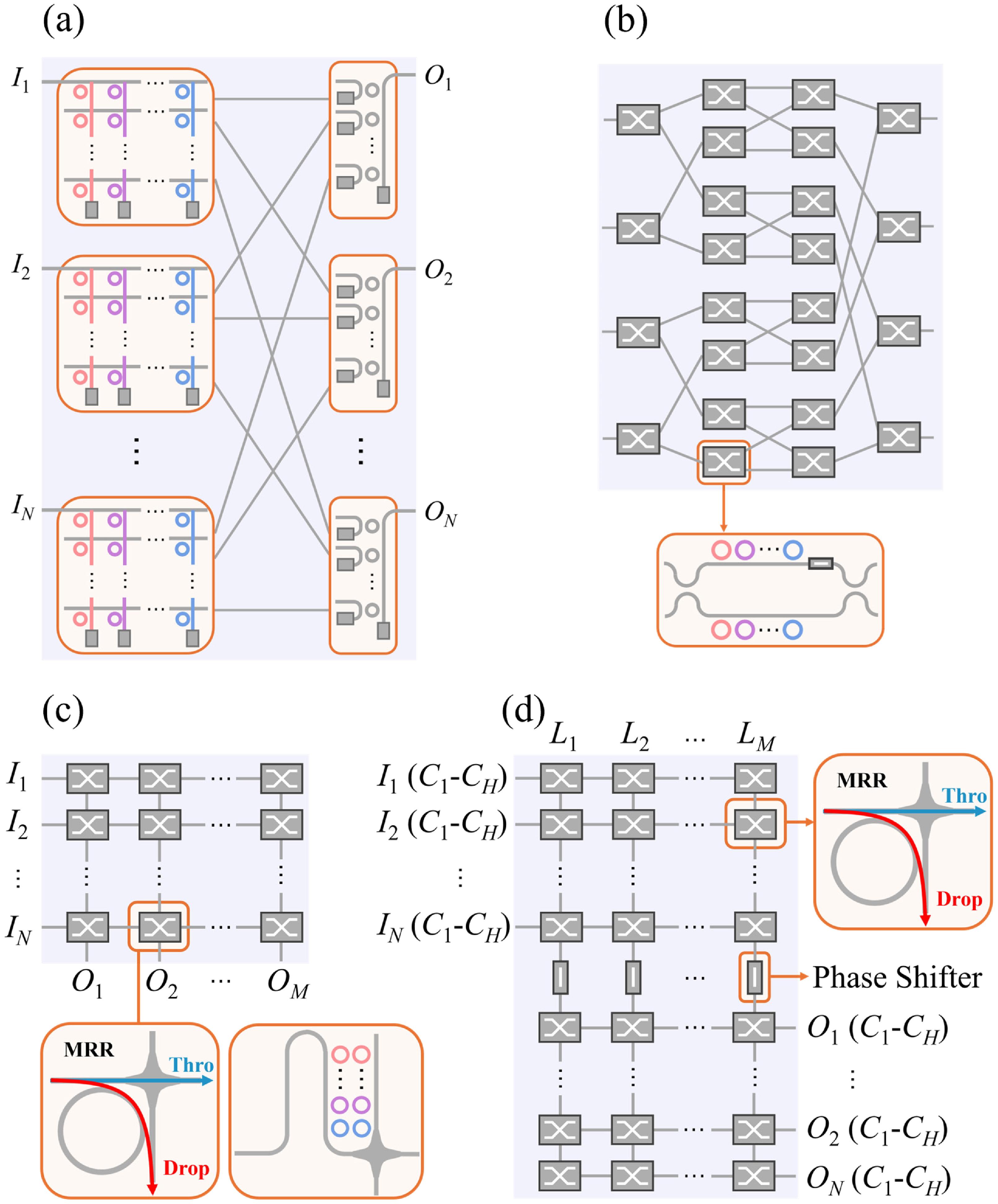
Photonic integrated switches that are both space and wavelength selective are a highly promising technology for data-intensive applications as they benefit from multi-dimensional manipulation of optical signals. However, scaling these switches normally poses stringent challenges such as increased fabrication complexity and control difficulties, due to the growing number of switching elements. In this work, we propose a new type of dilated crosspoint topology, which efficiently handles both space and wavelength selective switching, while reducing the required switching element count by an order of magnitude compared to reported designs. To the best of our knowledge, our design requires the fewest switching elements for an equivalent routing paths number and it fully cancels the first-order in-band crosstalk. We demonstrate such an ultra-compact space-and-wavelength selective switch (SWSS) at a scale of on the silicon-on-insulator (SOI) platform. Experimental results reveal that the switch achieves an insertion loss ranging from 2.3 dB to 8.6 dB and crosstalk levels in between and . The add-drop microring-resonators (MRRs) are equipped with micro-heaters, exhibiting a rise and fall time of 46 μs and 0.33 μs, respectively. These performance characteristics highlight the switch’s ultra-low element count and crosstalk with low insertion loss, making it a promising candidate for advanced data center applications.
Photonics Research
2025, 13(4): 924
1 清华大学深圳国际研究生院,广东 深圳 518055
2 重庆大学-辛辛那提大学联合学院,重庆 400044
3 清华-伯克利深圳学院,广东 深圳 518055
针对大深径比工件内孔参数测量困难的问题,提出一种基于光谱共焦原理的旋转测量方法。首先,设计并搭建大深径比内孔参数测量系统,将具有非接触测量功能的光谱共焦探头固定在空心长直导杆前端,导杆借助X-RX运动模组带动光谱共焦探头在孔深方向旋转前进。其次,根据不同的运动速度设置10组实验,分别采集光谱共焦探头在深度为222 mm、深径比为12.52的大深径比内孔工件中正反转交替各旋转3次的数据。最后,通过最小二乘法拟合内孔工件轮廓,提出求解孔内径、圆心坐标及垂直度的算法,并分析运动速度对内孔参数测量结果的影响。通过对比实验验证所提测量系统具有较高的测量精度:在低速情况下,孔内径测量值波动范围为±2 μm,垂直度在50 μm以内;在高速情况下,孔内径测量值波动范围为±7 μm,垂直度在80 μm以内。该结果与大深径比工件的标定值具有高度一致性,表明了所提方法与系统的有效性。
光谱共焦 内孔测量 非接触测量 最小二乘法 激光与光电子学进展
2025, 62(7): 0712003
西南科技大学信息工程学院,四川 绵阳 621010
目前,适用于近红外相机的标定设备的制作工艺较为复杂、昂贵,增加了光学外科导航系统的开发成本,同时,由于缺少可靠的特征点中心提取方法,导航系统的定位精度难以保证。基于此,参考了圆形标记点阵列靶标的硬件结构,使用灯珠设计了一种适用于近红外相机的标定设备,提出了一种具有唯一结果的排序方法,改进了椭圆拟合的方法。在提取特征点时,首先使用大津阈值法进行预处理,根据特征点的平均半径使用高斯核来减弱灯珠的散射光晕,然后基于Zernike矩检测特征点的亚像素边缘,并移除部分异常边缘,接着进行二次拟合,得到更为精确的特征点中心坐标,最后使用张氏标定法完成双目近红外相机的标定。实验结果表明,离群边缘移除后,重投影误差降低了约3%,双目重建的样本标准差下降了约3.3%。
光学外科导航系统 近红外相机标定设备 排序方法 亚像素边缘检测 离群边缘移除 激光与光电子学进展
2025, 62(6): 0615005
郑州工业应用技术学院 艺术设计学院,郑州 451150
针对LED光强分布不均导致室内可见光定位精度差异大的问题,结合序列到序列模型提出一种基于RSS指纹分析的室内可见光定位方法。将RSS指纹向量作为输入序列,室内三维空间坐标作为输出序列,采用序列到序列模型学习RSS指纹与室内三维空间之间的非线性映射关系。为序列到序列模型增加自注意力机制,利用自注意力机制分析RSS指纹中各元素对于不同位置的判别力高低,并在预测阶段调节各RSS元素的重要性。仿真结果表面,所提方法降低了不同信噪比条件下可见光定位的平均误差。
室内可见光 可见光通信 可见光定位 室内定位 深度学习 自注意力 indoor visible light visible light communication visible light positioning indoor positioning deep learning self attention
1 深圳大学微纳光电子学研究院,广东 深圳 518060
2 深圳技术大学工程物理学院,广东 深圳 518118
3 深圳大学电子信息与工程学院,广东 深圳 518060
4 深圳大学物理与光电工程学院,广东 深圳 518060
中红外波段柱矢量激光器在材料加工、粒子捕获、光学显微和存储等领域中具有广阔的应用前景。将飞秒激光刻写的自组织纳米结构光栅(S波片)作为偏振模式转换器件应用于全固态Er∶YAP激光器,实现了连续波和短脉冲可切换的中红外柱矢量激光高效输出,其中径向和角向偏振模式可快速切换。在连续波运转模式下获得了平均功率分别为136 mW和133 mW的径向偏振及角向偏振柱矢量激光输出,波长均为2.73 μm;基于光学斩波器实现了稳定的调Q脉冲柱矢量激光输出,最窄脉宽为124.73 ns,对应脉冲能量为13.84 μJ。这些研究结果为中红外结构光激光器的设计及实现提供了有益的参考。
中红外波段 柱矢量光 径向偏振光 角向偏振光 S波片 光学斩波器
Author Affiliations
Abstract
Sub-wavelength nanostructure lattices provide versatile platforms for light control and the basis for various novel phenomena and applications in physics, material science, chemistry, biology, and energy. The thriving study of nanostructure lattices is building on the remarkable progress of nanofabrication techniques, especially for the possibility of fabricating larger-area patterns while achieving higher-quality lattices, complex shapes, and hybrid materials units. In this review, we present a comprehensive review of techniques for large-area fabrication of optical nanostructure arrays, encompassing direct writing, self-assembly, controllable deposition, and nanoimprint/print methods. Furthermore, a particular focus is made on the recent improvement of unit accuracy and diversity, leading to integrated and multifunctional structures for devices and applications.
nanofabrication nanostructure lattices hybrid material structures metasurfaces large-area fabrication International Journal of Extreme Manufacturing
2024, 6(6): 062004
中国电子科技集团公司第二十六研究所,重庆 400060
引用CST三维电磁仿真软件提出了一种三阶介质滤波器的设计方法。通过源与第二谐振器或负载与第三谐振器构成级联三节(CT)交叉耦合结构产生传输零点的方式,满足更高频率端的高抑制要求。第二谐振器与第三谐振器开路端电极相连,形成三阶滤波器结构实现了低损耗性能。4个谐振器短路端被缩短,从而扩大了电极可调试区域以简化滤波器的调试复杂度。一体式介质滤波器采用介电常数为45.9的陶瓷材料制作样品并进行测试。测试结果表明,所设计的介质滤波器1 dB带宽为117 MHz,通带频率范围2 084~2 104 MHz的插入损耗(IL)小于1.2 dB,通带驻波比小于1.28,高端频率2.2 GHz处的衰减为34.35 dB,低端频率1.6 GHz处的抑制为31.04 dB,滤波器外形尺寸为10.41 mm×3.7 mm×4.57 mm。测试结果与仿真结果吻合度高。
耦合矩阵 电磁仿真软件CST 陶瓷介质滤波器 谐振器 交叉耦合结构 coupling matrix electromagnetic simulation software CST ceramic dielectric filter resonator cross-coupled structure
中国电子科技集团公司第二十六研究所,重庆 400060
传统的大功率腔体、LC滤波器体积较大,不符合在通信设备环境中器件小型化、轻量化的应用需求,因此设计了一款小体积、大功率介质滤波器。该滤波器采用具有高品质因数(Qf)值、高介电常数的微波陶瓷材料,在保持滤波器低损耗的前提下缩小其体积。采用三维场路联合仿真并结合参数提取的方法,缩短了设计周期。对功率容量进行分析,通过结构的改进提升了最大场强处介质抗击穿强度,提高了承受高功率脉冲的能力。对所设计的样品进行测试,测试结果表明,在S波段相对带宽14.5%内,带内插损小于0.7 dB,在近端频率点2 690 MHz处,抑制大于22 dB;在频率3 600~4 200 MHz内,抑制大于32 dB,可通过超10 W的功率信号。该介质滤波器尺寸为23 mm×10 mm×10 mm,能够应用于大功率通信系统环境中。
联合仿真 参数提取 大功率 脉冲 介质滤波器 co-simulation parameter extraction high power pulse dielectric filter
1 重庆邮电大学,重庆 400700
2 中国科学院重庆绿色智能技术研究院,重庆 400714
硫化铅(PbS)等铅盐材料因较低的俄歇复合系数,是非制冷红外探测领域中备受关注的材料。化学水浴法被广泛用于硫化铅等薄膜的制备。然而该方法在图形化衬底上存在薄膜生长不均匀的问题。基于多次曝光显影技术,比较了不同预处理工艺对图形化衬底上薄膜生长均匀性的影响,在金属和绝缘衬底表面上均实现了硫化铅薄膜的均匀生长。基于优选预处理方法制备的硫化铅探测器的结果表明,图形衬底预处理可明显改善探测器在光电流、响应度和噪声等方面的性能,其中响应度可提升1.2倍。本文提供的硫化铅薄膜制备方法,不仅可在图形化衬底上生长均匀性一致的硫化铅薄膜,还可以修复受损衬底,有利于在读出电路表面实现硫化铅基焦平面阵列探测器的一体化加工。
化学水浴法 硫化铅 生长均匀性 光电探测器 红外探测器 chemical bath deposition method lead sulfide growth uniformity photodetector infrared detector


