红外与激光工程, 2020, 49 (12): 20201057, 网络出版: 2021-01-14
飞秒激光诱导金刚石微纳结构及其应用(特邀)  下载: 544次
Femtosecond laser induced microstructures in diamond and applications (Invited)
图 & 表
图 1. Schematic diagram of the crystal structure of diamond with NV center (carbon atoms represented in black, nitrogen atom shown in yellow, and the vacancy shown in white)[23]氮空位中心的金刚石晶体结构示意图(碳原子用黑色表示,氮原子用黄色表示,空位用白色表示)[23]
Fig. 1.
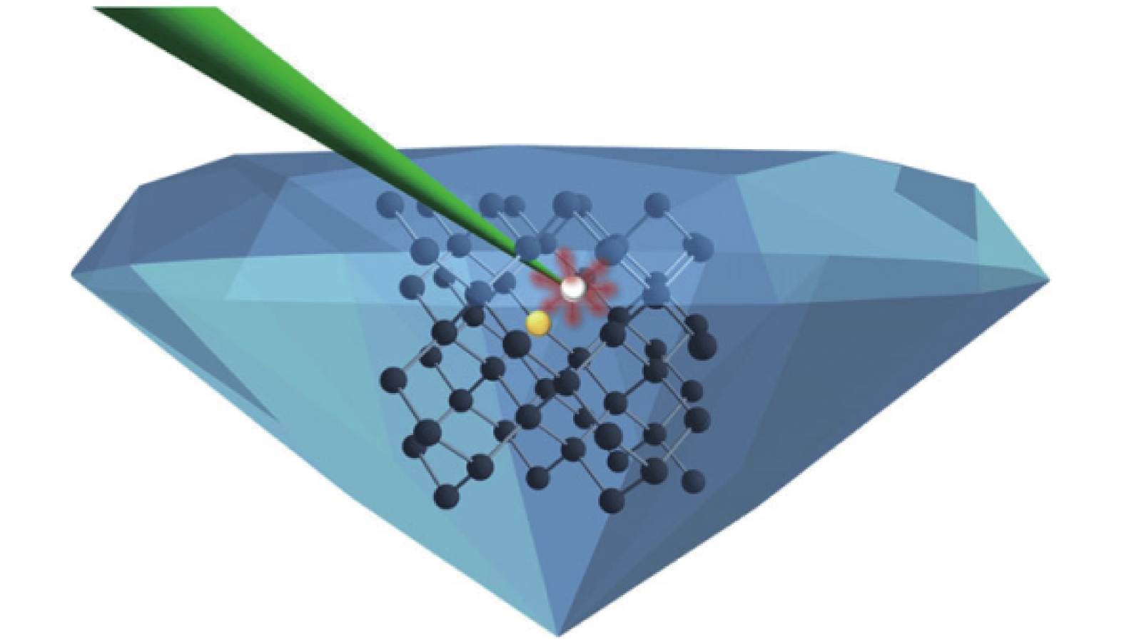
图 2. (a) Experimental setup for the femtosecond laser illumination on a diamond sample; (b) Illuminated diamond sample by femtosecond pulsed laser with different illumination time; (c) Same diamond sample after slow oxidation[26](a)飞秒激光实验装置;(b)不同辐照时间下的飞秒脉冲激光辐照金刚石表面样品图片;(c)氧化后的金刚石样品[26]
Fig. 2.

图 3. Schematic of the laser-writing process. A single seed pulse is used to generate vacancies in the crystal, followed by a pulse train at lower energy to locally anneal the diamond[30]激光直写过程原理图。单脉冲在晶体中产生空位,然后以较低能量的脉冲序列对金刚石进行局部退火[30]
Fig. 3.

图 4. (a) Transverse optical microscope image of single laser-induced track written with 500 kHz repetition rate. 50 mW average power and 0.5 mm/s scan speed; (b) μ-Raman spectra (532 nm excitation wavelength) at four different vertical positions inside the modifcation. "Out" refers to a spectrum taken outside the track. The spectra have been normalized to the diamond peak to show the change in the relative intensity of the G-peak inside the structure[31]500 kHz重复频率下抑制辐照区域产生石墨。(a)辐照区域截面光学显微照片,重复频率为500 kHz,平均功率50 mW,扫描速度0.5 mm/s;(b) 辐照区域垂直的四个点上μ-Raman光谱(532 nm波长激发),Out指的是辐照区域外的拉曼光谱。光谱已归一化到金刚石峰,以显示结构内部G峰的相对强度的变化[31]
Fig. 4.

图 5. Shift of the Raman diamond peak at the center for different repetition rates [32]不同重复频率下特征峰中心位置的偏移[32]
Fig. 5.

图 6. (a) Map of the refractive index profile; (b) Measured vertical line profile of τ 1 and τ 2 at the center of the waveguide[33](a)折射率分布图;(b)沿波导中心垂直线方向纵断面应力τ 1和τ 2测量数据[33]
Fig. 6.

图 7. Top (xy ) and side (xz ) view of the date fabricated in diamond at a depth of 80 μm. (a) Without aberration correction; (b) Employing the dual adaptive optics system. The laser beam was incident along the z direction, the scale bar represents 5 μm[35]金刚石内部距表面80 μm激光直写数字日期的俯视(xy )和侧视(xz )照片。(a)没有像差校正;(b)采用双重自适应光学系统。激光束沿z 方向入射,标尺长度5 μm[35]
Fig. 7.

图 8. μ-Raman spectra (normalized to the G-peak) in the center of modification tracks at repetition rates of 5 kHz, 25 kHz and 500 kHz, with pulse energy held constant (800 nJ) to produce a similar size modification at each repetition rate[31]重复频率为5 kHz,25 kHz和500 kHz激光光辐照区域拉曼光谱(G峰归一化处理),脉冲能量保持不变(800 nJ),在每个位置产生类似辐照区域的尺寸[31]
Fig. 8.

图 9. Transverse microscope view of type II waveguide in diamond along with near field mode profile (λ =635 nm). An arrow indicates the position of the mode[31]II型波导的横向显微镜视图及近场模场剖面图(λ = 635 nm),箭头指向对应模场在双线波导位置[31]
Fig. 9.

图 10. Interferometric autocorrelations of the 150 MHz pulse trains generated by the KLM Cr:ZnSe at the input facet of the diamond crystal (a); At the waveguide output (b); After propagation through bulk diamond crystal (c). The red, blue, and green curves in the autocorrelations correspond to the intensity autocorrelation profile(a)输入端由克尔自锁模Cr:ZnSe激光器输入脉冲频率为150 MHz的脉冲串后的自相关曲线; (b)波导输出端自相关曲线;(c)金刚石样品输出端自相关曲线,红、蓝、绿曲线为对应于密度的自相关曲线
Fig. 10.

图 11. End-facet of the type III depressed cladding waveguides, over layered with the measured guided near-field mode profile for a core diameter of 20 µm and 25 µm[41]直径20 µm和25 µm的Ⅲ型凹陷包层波导端面,测量的波导近场模式剖面分层图[41]
Fig. 11.

图 12. (a) Histogram showing g (2)(δt ) from a single NV centre;(b) Histogram of g (2)(0) for the different laser processing sites, allowing the identification of sites of single, double and triple NV centre generation[29](a)单NV色心g (2)(δt )的直方图; (b) 针对不同的激光加工位点,可识别位点是产生了单、双或三重NV色心及其g (2)(0)值分布图[29]
Fig. 12.

图 13. (a) NV− color center fluorescence spectrum and fluorescence monitor band; (b) Histogram of g (2)(0) values for the array; (Inset) typical g (2)(τ ) dataset corrected for background signal from the bulk crystal[30](a) NV−色心荧光光谱和荧光波段;(b) g (2)(0)值分布图,插入图为修正晶体背景信号后典型g (2)(τ )曲线图[30]
Fig. 13.

图 14. Second-order autocorrelation functions of the PL from SiV− A and B with background noise correction, revealing single SiV− centers[27]经过背景噪声校正的来自SiV-的二阶自相关函数,其特征值显示单SiV-色心[27]
Fig. 14.

图 15. Optical images of the detector. The metallization and readout strips are shown in gold. The three areas are: left, planar array; middle, 3D phantom array; right, 3D array. The detector connection scheme with bias voltage (HV) contacted to the back side, and channel 1 (CH1) and channel 2 (CH2) connected to the current amplifiers is shown. The areas enclosed in the dashed line correspond to the measurement locations[37]探测器的光学照片。金属导线和引脚显示为金色。三块区域:左边是平面阵列;中间是平面化阵列;右边是三维阵列。探测器的连接方案,偏置电压(HV)加载在后端与通道1 (CH1)、连接到电流放大器的通道2 (CH2)。虚线包围的区域对应于测量位置[37]
Fig. 15.


王华丰, 孙轲, 孙盛芝, 邱建荣. 飞秒激光诱导金刚石微纳结构及其应用(特邀)[J]. 红外与激光工程, 2020, 49(12): 20201057. Huafeng Wang, Ke Sun, Shengzhi Sun, Jianrong Qiu. Femtosecond laser induced microstructures in diamond and applications (Invited)[J]. Infrared and Laser Engineering, 2020, 49(12): 20201057.


 PDF全文
PDF全文
