Photonics Research, 2020, 8 (4): 04000457, Published Online: Mar. 12, 2020
Optimizing an interleaved p-n junction to reduce energy dissipation in silicon slow-light modulators  Download: 519次
Figures & Tables
Fig. 1. Schematic of the slow-light waveguide with definition of the structure (a) in 3D and (b) in top view with grating parameters and (c) doping profiles. The silicon material in (a) and (b) (orange) is fully embedded in SiO 2
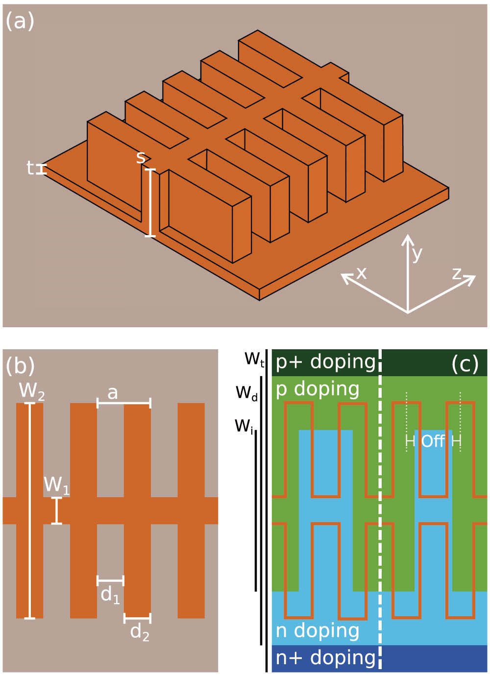
Fig. 2. Group index (left scale) and propagation loss per unit length at zero bias (right scale) as a function of wavelength. Parameters: see discussion in Section 2 , in particular W i = 0.6 μm N = P = 8 × 10 17 cm − 3 O f f = 0

Fig. 3. (a) Capacitance per unit length (left scale) and resistance times length (right scale). (b) 3 dB cutoff frequency as a function of reverse voltage. Parameters: see discussion in Section 2 , in particular W i = 0.6 μm N = P = 8 × 10 17 cm − 3 O f f = 0

Fig. 4. (Upper panels) V π L π L π

Fig. 5. (a), (b) Charge densities for V = 0 V V = 1 V λ = 1.315 μm a = 0.234 μm z

Fig. 6. (a) Schematic structure of a Mach–Zehnder interferometer and (b) output power as a function of the phase difference between the arms (with definition of the quadrature working point): solid, P out P ¯ out

Fig. 7. (a) Transmission spectrum and (b) extinction ratio and total loss of an MZ modulator with length 0.5 mm and bias 1 V.

Fig. 8. Normalized OMA as a function of wavelength for different modulator lengths and applied voltages.

Fig. 9. Minimum normalized OMA level as a function of modulator length, for different bandwidths (bw) and applied voltages. Upper panels: slow-light waveguide with interleaved p-n junction. Lower panels: rib waveguide with interleaved p-n junction, notice that the three curves with bw = 10 x E bit = C V 2 / 2

Fig. 10. (a) Normalized OMA as a function of wavelength for an L = 0.5 mm x 9 . The reverse applied voltage is V = 1 V

Fig. 11. Various figures of merit: capacitance per unit length, resistance times length, 3 dB cutoff frequency, V π L π ( L π ) λ = 1.315 μm W i = 0.6 μm O f f = 0 N = P = 8 × 10 17 cm − 3 O f f = 0 N = P = 8 × 10 17 cm − 3 W i = 0.6 μm V = 0 V V = 1 V V = 2 V V = 3 V

Marco Passoni, Dario Gerace, Liam O’Faolain, Lucio Claudio Andreani. Optimizing an interleaved p-n junction to reduce energy dissipation in silicon slow-light modulators[J]. Photonics Research, 2020, 8(4): 04000457.


 PDF全文
PDF全文

