Photonics Research, 2019, 7 (5): 05000586, Published Online: May. 5, 2019
Dual-band and ultra-broadband photonic spin-orbit interaction for electromagnetic shaping based on single-layer silicon metasurfaces Download: 580次
Figures & Tables
Fig. 1. Schematic of the scattering engineered metasurface with a chessboard-like configuration; λ 1 and λ 2 denote the incoming wavelengths from two infrared bands. Inset illustrates the super cell of the metasurface.
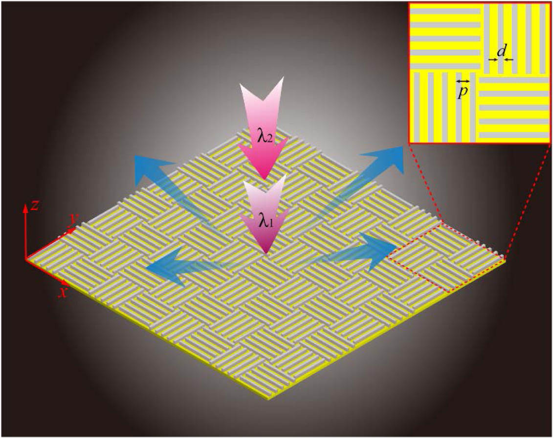
Fig. 2. Numerically calculated results of the (a)–(g) dual-band and (h)–(m) ultra-broadband unit cells. (a) Schematic view of a periodic α -Si ridge array on a gold mirror. (b) Reflection phase for the unit cells under x - (TM) and y - (TE) polarized incidences, as well as the relative phase difference between x and y polarizations. (c) Cross-polarization and co-polarization reflectances under circularly polarized illumination at near-infrared and far-infrared spectra. (d), (e) Calculated (d) electric field distributions and (e) phase profiles for TE- and TM-polarized illuminations at 1.06 μm. (f), (g) Calculated (f) electric field distributions and (g) phase profiles for TE- and TM-polarized illuminations at 10.6 μm. (h) Ultra-broadband cross-polarization and co-polarization reflectances under circularly polarized illumination. (i), (j) Calculated (i) reflectance and (j) phase for TE and TM illuminations. (k) Phase difference between the two orthogonal polarizations. (l) Phase distributions for TM illumination at 49 THz and 50 THz. (m) Magnetic field profiles for TM illumination at 49 THz and 50 THz.
Fig. 3. Full-wave simulations for the (a)–(f) dual-band and (g)–(k) ultra-broadband metasurfaces for x -polarized normal incidences. (a), (b) 3D scattering patterns of the dual-band metasurface at 1.06 μm and 10.6 μm, respectively. (c), (d) Scattering patterns of the dual-band metasurface on φ = 45 ° plane at 1.06 μm and 10.6 μm, respectively. (e), (f) Calculated specular reflectance spectra of the dual-band metasurface and an Au plate. (g), (h) 3D scattering patterns of the ultra-broadband metasurface at 5 μm and 12 μm, respectively. (i), (j) Scattering patterns of the ultra-broadband metasurface on φ = 45 ° plane at 5 μm and 12 μm, respectively. (k) Calculated specular reflectance spectra of the ultra-broadband metasurface and an Au plate.
Fig. 4. Sample fabrication and measurements. (a) Schematic of the fabrication process. (b) SEM image of part of the fabricated metasurface. Scale bar: 50 μm. (c) Measured reflectance spectra of the fabricated sample and Au plate under oblique incidences. (d) Measured thermal infrared images of a ceramic doll, a gold plate, and the fabricated sample. The white dotted frame marks the fabricated area.
Fig. 5. Simulated electric field magnitude distributions E x in the gap between two α -Si ridges under x -polarized illumination and the catenary curves fitting at the wavelength of (a) 1.06 μm and (b) 10.6 μm, respectively.
Fig. 6. Full-wave simulated specular reflectance spectra of the metasurface under oblique incidences of (a) 15°, (b) 20°, and (c) 30°, respectively.
Xin Xie, Mingbo Pu, Xiong Li, Kaipeng Liu, Jinjin Jin, Xiaoliang Ma, Xiangang Luo. Dual-band and ultra-broadband photonic spin-orbit interaction for electromagnetic shaping based on single-layer silicon metasurfaces[J]. Photonics Research, 2019, 7(5): 05000586.