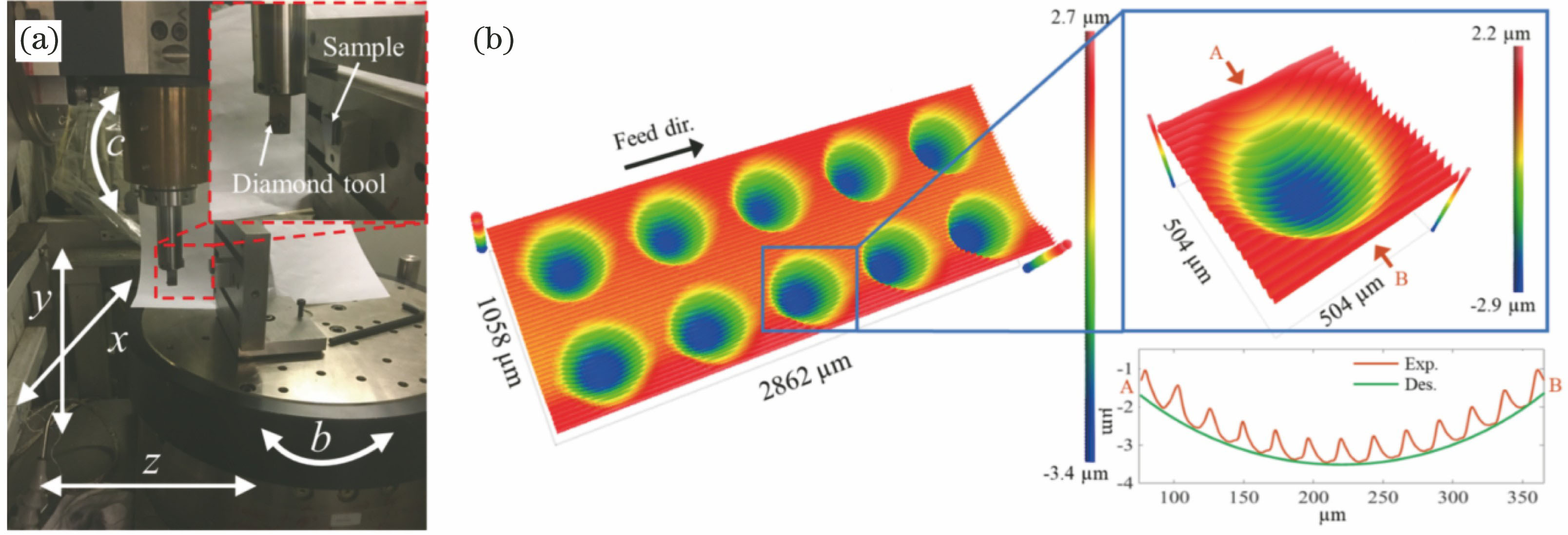
折射型红外微透镜阵列器件的发展及制备  下载: 2605次特邀综述
刘丰, 张帆, 边浩, 杨青, 李敏静, 陈烽. 折射型红外微透镜阵列器件的发展及制备[J]. 激光与光电子学进展, 2020, 57(7): 071607.
Feng Liu, Fan Zhang, Hao Bian, Qing Yang, Minjing Li, Feng Chen. Development and Preparation of Refractive Infrared Microlens Array Device[J]. Laser & Optoelectronics Progress, 2020, 57(7): 071607.
[1] Ting D Z, Soibel A, Khoshakhlagh A, et al. Advances in III-V semiconductor infrared absorbers and detectors[J]. Infrared Physics & Technology, 2019, 97: 210-216.
[2] Rogalski A. Next decade in infrared detectors[J]. Proceedings of SPIE, 2017, 10433: 104330L.
[3] Tu X C, Xiao P, Kang L, et al. Nb5N6 microbolometer for sensitive, fast-response, 2-μm detection[J]. Optics Express, 2018, 26(12): 15585-15593.
[5] Cha D H, Kim H J, Park H S, et al. Effect of temperature on the molding of chalcogenide glass lenses for infrared imaging applications[J]. Applied Optics, 2010, 49(9): 1607-1613.
[6] Franks J. Molded, wafer level optics for long wave infrared applications[J]. Proceedings of SPIE, 2016, 9822: 98220B.
[7] Xie H B, Zhao M, Wang Y, et al. Switchable FoV infrared imaging system using micro-lens arrays[J]. OSA Continuum, 2019, 2(6): 1925-1937.
[8] Xie D, Song Y, Song Y, et al. Design of a micro uncooled infrared imaging system based on VOx IRFPA[J]. Proceedings of SPIE, 2016, 10025: 1002516.
[10] MaxtechInternational, Inc. Volume IRW-M: the world market for military infrared imaging detectors & systems[R]. Sarasota, FL, USA: Maxtech International, Inc., 2019.
[14] Banerji S, Meem M, Majumder A, et al. Imaging with flat optics: metalenses or diffractive lenses?[J]. Optica, 2019, 6(6): 805-810.
[15] Liu M Z, Fan Q B, Yu L, et al. Polarization-independent infrared micro-lens array based on all-silicon metasurfaces[J]. Optics Express, 2019, 27(8): 10738-10744.
[21] Adam JL, ZhangX. Chalcogenide glasses: Preparation, properties and applications[M]. Cambridge: Woodhead Publishing Limited, 2014.
[22] Gan F X. Structure, properties and applications of chalcohalide glasses: a review[J]. Journal of Non-Crystalline Solids, 1992, 140: 184-193.
[23] Xu H J, He Y J, Wang X S, et al. Preparation of low-loss Ge15Ga10Te75 chalcogenide glass for far-IR optics applications[J]. Infrared Physics & Technology, 2014, 65: 77-82.
[24] Kitamura R, Pilon L, Jonasz M. Optical constants of silica glass from extreme ultraviolet to far infrared at near room temperature[J]. Applied Optics, 2007, 46(33): 8118-8133.
[25] Thomas M E, Joseph R I, Tropf W J. Infrared transmission properties of sapphire, spinel, yttria, and ALON as a function of temperature and frequency[J]. Applied Optics, 1988, 27(2): 239-245.
[28] Liu X Q, Yang S N, Yu L, et al. Rapid engraving of artificial compound eyes from curved sapphire substrate[J]. Advanced Functional Materials, 2019, 29(18): 1900037.
[29] Cao X W, Lu Y M, Fan H, et al. Wet-etching-assisted femtosecond laser holographic processing of a sapphire concavemicrolens array[J]. Applied Optics, 2018, 57(32): 9604-9608.
[30] Cao X W, Chen Q D, Zhang L, et al. Single-pulse writing of a concave microlens array[J]. Optics Letters, 2018, 43(4): 831-834.
[31] Liu F, Yang Q, Bian H, et al. Artificial compound eye-tipped optical fiber for wide field illumination[J]. Optics Letters, 2019, 44(24): 5961-5964.
[34] Zhang F, Wang C, Yin K, et al. Quasi-periodic concave microlens array for liquid refractive index sensing fabricated by femtosecond laser assisted with chemical etching[J]. Scientific Reports, 2018, 8: 2419.
[35] Wei Y, Yang Q, Bian H, et al. Fabrication of high integrated microlens arrays on a glass substrate for 3D micro-optical systems[J]. Applied Surface Science, 2018, 457: 1202-1207.
[36] Deng Z F, Chen F, Yang Q, et al. Dragonfly-eye-inspired artificial compound eyes with sophisticated imaging[J]. Advanced Functional Materials, 2016, 26(12): 1995-2001.
[37] Bian H, Wei Y, Yang Q, et al. Direct fabrication of compound-eye microlens array on curved surfaces by a facile femtosecond laser enhanced wet etching process[J]. Applied Physics Letters, 2016, 109(22): 221109.
[38] BrettinA, AbolmaaliF, Limberopoulos NI, et al. Towards fabrication of mid-IR FPAs with enhanced sensitivity and reduced dark current by using integration with microspherical arrays[C]∥NAECON 2018-IEEE National Aerospace and Electronics Conference, July 23-26, 2018. Dayton, OH. New York: IEEE, 2018: 533- 535.
[39] Mukaida M, Yan J W. Ductile machining of single-crystal silicon for microlens arrays by ultraprecision diamond turning using a slow tool servo[J]. International Journal of Machine Tools & Manufacture, 2017, 115: 2-14.
[40] Sun Z W, To S, Yu K M. One-step generation of hybrid micro-optics with high-frequency diffractive structures on infrared materials by ultra-precision side milling[J]. Optics Express, 2018, 26(21): 28161-28177.
[41] Zhang L, Zhou W C, Naples N J, et al. Fabrication of an infrared Shack-Hartmann sensor by combining high-speed single-point diamond milling and precision compression molding processes[J]. Applied Optics, 2018, 57(13): 3598-3605.
[42] Liu X H, Zhou T F, Zhang L, et al. Fabrication of spherical microlens array by combining lapping on silicon wafer and rapid surface molding[J]. Journal of Micromechanics and Microengineering, 2018, 28(7): 075008.
[43] Hahn C, Amyot-Bourgeois M, Al-Shehab M, et al. Nanofabrication of plasmonic structures on insulating substrates by resist-on-metal bilayer lift-off[J]. Nanotechnology, 2019, 30(5): 054003.
[45] Kumaresan Y, Rammohan A, Dwivedi P K, et al. Large area IR microlens arrays of chalcogenide glass photoresists by grayscale maskless lithography[J]. ACS Applied Materials & Interfaces, 2013, 5(15): 7094-7100.
[46] Fan P X, Bai B F, Zhong M L, et al. General strategy toward dual-scale-controlled metallic micro-nano hybrid structures with ultralow reflectance[J]. ACS Nano, 2017, 11(7): 7401-7408.
[47] Tan Y X, Chu W, Lin J T, et al. Metal surface structuring with spatiotemporally focused femtosecond laser pulses[J]. Journal of Optics, 2018, 20(1): 014010.
[48] Li Y P, Zhang T H, Fan S L, et al. Fabrication of micro hole array on the surface of CVD ZnS by scanning ultrafast pulse laser for antireflection[J]. Optical Materials, 2017, 66: 356-360.
[50] Peng L F, Deng Y J, Yi P Y, et al. Micro hot embossing of thermoplastic polymers: a review[J]. Journal of Micromechanics and Microengineering, 2014, 24(1): 013001.
[51] Liu F, Yang Q, Chen F, et al. Low-cost high integration IR polymermicrolens array[J]. Optics Letters, 2019, 44(7): 1600-1602.
[52] Liu F, Bian H, Zhang F, et al. IR artificial compound eye[J]. Advanced Optical Materials, 2019, 1901767.
[53] Aktaş O. Chalcogenide microresonators tailored to distinct morphologies by the shaping of glasses on silica tapers[J]. Optics Letters, 2017, 42(5): 907-910.
[54] Qiu J F, Li M J, Ye H C, et al. Fabrication of high fill-factor microlens array using spatially constrained thermal reflow[J]. Sensors and Actuators A: Physical, 2018, 279: 17-26.
[55] Yamazaki R, Obana A, Kimata M. Microlens for uncooled infrared array sensor[J]. Electronics and Communications in Japan, 2013, 96(2): 42-47.
[58] Robbins H, Schwartz B. Chemical etching of silicon II[J]. Journal of the Electrochemical Society, 1960, 107(2): 108-111.
[59] Meng X W, Chen F, Yang Q, et al. Simple fabrication of closed-packed IR microlens arrays on silicon by femtosecond laser wet etching[J]. Applied Physics A, 2015, 121(1): 157-162.
[60] Deng Z F, Yang Q, Chen F, et al. Fabrication of large-area concavemicrolens array on silicon by femtosecond laser micromachining[J]. Optics Letters, 2015, 40(9): 1928-1931.
[61] Gai X, Han T, Prasad A, et al. Progress in optical waveguides fabricated from chalcogenide glasses[J]. Optics Express, 2010, 18(25): 26635-26646.
[62] Mamedov S B, Mikhailov M D. Dissolution kinetics of glassy and crystalline As2S3 in aqueous sodium sulfide and hydroxide[J]. Journal of Non-Crystalline Solids, 1997, 221(2/3): 181-186.
[63] Antoine K, Jain H, Vlcek M. Optical spectroscopy of a-As2Se3 under in situ laser irradiation[J]. Journal of Non-Crystalline Solids, 2006, 352(6/7): 595-600.
[64] Zhou W C, Zhang L, Yi A Y. Design and fabrication of a compound-eye system using precision molded chalcogenide glass freeform microlens arrays[J]. Optik, 2018, 171: 294-303.
[65] D'Amico C. Caillaud C, Velpula P K, et al. Ultrafast laser-induced refractive index changes in Ge15As15S70 chalcogenide glass[J]. Optical Materials Express, 2016, 6(6): 1914-1928.
[66] Kuzma V, Bilanych V, Kozejova M, et al. Study of dependence of electron beam induced surface relief formation on Ge-As-Se thin films on the film elemental composition[J]. Journal of Non-Crystalline Solids, 2017, 456: 7-11.
[67] Clemens P C. Reversible optical storage on a low-doped Te-based chalcogenide film with a capping layer[J]. Applied Optics, 1983, 22(20): 3165-3168.
[68] Kadan V, Blonskyi I, Shynkarenko Y, et al. Single-pulse femtosecond laser fabrication of concave microlens-and micromirror arrays in chalcohalide glass[J]. Optics & Laser Technology, 2017, 96: 283-289.
[70] Xin Z W, Wei D, Chen M C, et al. Graphene-based adaptive liquid-crystal microlens array for a wide infrared spectral region[J]. Optical Materials Express, 2019, 9(1): 183-194.
[71] Lasers and laser-relatedequipment. ISO 21254-2: 2011[S]. Switzerland: ISO Copyright Office, 2011.
[72] Brady D J, Gehm M E, Stack R A, et al. Multiscale gigapixel photography[J]. Nature, 2012, 486(7403): 386-389.
[73] Ma Z C, Hu X Y, Zhang Y L, et al. Smart compound eyes enable tunable imaging[J]. Advanced Functional Materials, 2019, 29(38): 1903340.
[74] Xu Q, Dai B, Jiao Z A, et al. Fabrication of large micro-structured high-numerical-aperture optofluidic compound eyes with tunable angle of view[J]. Optics Express, 2018, 26(25): 33356.
[75] Shi C Y, Wang Y Y, Liu C Y, et al. SCECam: a spherical compound eye camera for fast location and recognition of objects at a large field of view[J]. Optics Express, 2017, 25(26): 32333-32345.
[76] Boyd D A, Nguyen V Q. McClain C C, et al. Optical properties of a sulfur-rich organically modified chalcogenide polymer synthesized via inverse vulcanization and containing an organometallic comonomer[J]. ACS Macro Letters, 2019, 8(2): 113-116.
[77] Babaeian M, Diaz L R, Namnabat S, et al. Nonlinear optical properties of chalcogenide hybrid inorganic/organic polymers (CHIPs) using the Z-scan technique[J]. Optical Materials Express, 2018, 8(9): 2510-2519.
[80] Zhang L, Ma X, Zhuang J, et al. Microfabrication of a diffractive microlens array on n-GaAs by an efficient electrochemical method[J]. Advanced Materials, 2007, 19(22): 3912-3918.
[81] Zhang S Y, Soibel A, Keo S A, et al. Solid-immersion metalenses for infrared focal plane arrays[J]. Applied Physics Letters, 2018, 113(11): 111104.
[82] Fan D J, Lee B, Coburn C, et al. From 2D to 3D: strain-and elongation-free topological transformations of optoelectronic circuits[J]. Proceedings of the National Academy of Sciences of the United States of America, 2019, 116(10): 3968-3973.
[83] Zhang K, Jung Y H, Mikael S, et al. Origami silicon optoelectronics for hemispherical electronic eye systems[J]. Nature Communications, 2017, 8: 1782.
[84] Gui Y, Chen H R, Yang B, et al. Flexible omega-ring metamaterial sensor with ultrahigh sensitivity in the terahertz region[J]. Optical Materials Express, 2017, 7(11): 4123-4130.
刘丰, 张帆, 边浩, 杨青, 李敏静, 陈烽. 折射型红外微透镜阵列器件的发展及制备[J]. 激光与光电子学进展, 2020, 57(7): 071607. Feng Liu, Fan Zhang, Hao Bian, Qing Yang, Minjing Li, Feng Chen. Development and Preparation of Refractive Infrared Microlens Array Device[J]. Laser & Optoelectronics Progress, 2020, 57(7): 071607.


