天津工业大学 电子与信息工程学院, 天津 300000
低半波电压电光调制器是实现大规模光电集成的关键。文章提出了一种半波电压低于1.5V的薄膜铌酸锂马赫-曾德尔(Mach-Zehnder,MZ)电光调制器,选用绝缘体上单晶薄膜铌酸锂材料作为设计基础,分析了直波导、多模干涉耦合器、弯曲波导和调制臂等结构对电光调制器的影响。结果表明,当调制臂长为3mm时,该薄膜铌酸锂电光调制器具有1.05V的低半波电压、0.319dB的低损耗和27dB的高消光比。同时,该调制器半波电压长度积为0.315V·cm,调制效率高,具有与CMOS技术兼容的半波电压,有利于大规模光电集成。
铌酸锂 马赫-曾德尔电光调制器 多模干涉耦合器 低半波电压 lithium niobate Mach-Zehnder electro-optic modulators multimode interference couplers low half-wave voltage
1 宁波大学信息科学与工程学院,浙江 宁波 315211
2 浙江大学光电科学与工程学院,浙江 杭州 310058
3 浙江万里学院数字产业研究院,浙江 宁波 315100
光子集成技术的高速发展对功能器件的设计效率提出了较高的要求。逆向设计利用优化算法实现器件结构的智能设计,从而可有效降低设计复杂度,提升设计效率。利用基于伴随法的逆向设计算法对硅基平台上的光耦合器进行结构设计,通过优化器件的边界形状,实现了高效率、任意分光比输出。仿真验证了三种1×2光耦合器的性能,其分光比分别为1∶2、1∶4和1∶8(3 dB、6 dB和9 dB)。器件的设计尺寸仅为4 μm×2 μm,且可以通过一步刻蚀完成。在1550 nm波长处,所设计的耦合器均可达到设计目标,且最大插入损耗仅有0.12 dB。在1500~1600 nm波长范围内,三种耦合器的分光比相对于设计目标的误差均保持在±1 dB以内,并且三种耦合器的插入损耗均低于0.28 dB。针对制作工艺误差等问题,对器件的制作容差进行了分析。结果表明,当耦合器的整体宽度变化±20 nm时,三种耦合器在1550 nm波长处的分光比的误差仍能保持在±1 dB以内。此外,制造了分光比为1∶2的耦合器,且实验结果符合设计目标。
集成光学 全光器件 耦合器 逆向设计
1 西安理工大学自动化与信息工程学院, 陕西 西安 710048
2 西安工业大学光电工程学院, 陕西 西安 710021
光纤与平面光波导高效耦合是光波导器件互联设计中的重要环节,常用的倒锥波导已经解决了光纤与波导芯片之间的模式不匹配问题。然而,高折射率差波导与光纤耦合时通常需要较小的尖端尺寸(<180 nm),加工复杂且波导易坍塌。设计了一种宽波段(可见光和近红外波段)光纤-波导水平耦合器,通过引入聚合物SU-8锥形结构,提高了三端口分支波导的线宽,实现了850 nm波段超过300 nm的1 dB有效带宽。
集成光学 耦合器 波导 光通信 聚合物波导
特种光纤与光接入网重点实验室,特种光纤与先进通信国际合作联合实验室,上海先进通信与数据科学研究院,上海大学,上海 200444
本文提出了一种可以实现光纤高阶模式(HOM)在激光腔内振荡的锁模掺镱光纤激光器。通过使用一对级联的模式选择耦合器(MSC)作为有效的模式转换器,获得光纤锁模激光腔内HOM产生。其中,制备的MSC中心波长为1064 nm,可实现80 nm的模式转换带宽和94%的高阶模式纯度。通过搭建掺镱锁模光纤激光器,实验获得了3 dB谱宽7.4 nm、脉冲重复频率10.9 MHz、射频信噪比55 dB的锁模脉冲激光,输出功率的斜率效率为2.3%。实验证明,这种方法可在激光器内部通过模式级联转换,且能参与腔内锁模过程获得脉冲HOM激光。
模式选择耦合器 高阶模式 掺镱光纤 锁模光纤激光器 mode-selective couplers high-order mode Yb-doped fibers mode-locking fiber lasers

Author Affiliations
Abstract
1 State Key Laboratory on Integrated Optoelectronics, Institute of Semiconductors, Chinese Academy of Science, Beijing 100083, China
2 College of Materials Science and Opto-Electronic Technology, University of Chinese Academy of Sciences, Beijing 100083, China
In this Letter, a 16 channel 200 GHz wavelength tunable arrayed waveguide grating (AWG) is designed and fabricated based on the silicon on insulator platform. Considering that the performance of the AWG, such as central wavelength and crosstalk, is sensitive to the dimension variation of waveguides, the error analysis of the AWG with width fluctuations is worked out using the transfer function method. A heater is designed to realize the wavelength tunability of the AWG based on the thermo-optic effect of silicon. The measured results show that the insertion loss of the AWG is about 6 dB, and the crosstalk is 7.5 dB. The wavelength tunability of 1.1 nm is achieved at 276 mW power consumption, and more wavelength shifts will gain at larger power consumption.
060.1810 Buffers, couplers, routers,switches, and multiplexers 060.4230 Multiplexing 230.7390 Waveguides, planar Chinese Optics Letters
2018, 16(1): 010601
Author Affiliations
Abstract
1 College of Science, Zhejiang University of Technology, Hangzhou 310023, China
2 Institute for Information Recording of NAS of Ukraine, Shpak Str. 2, Kiev 03113, Ukraine
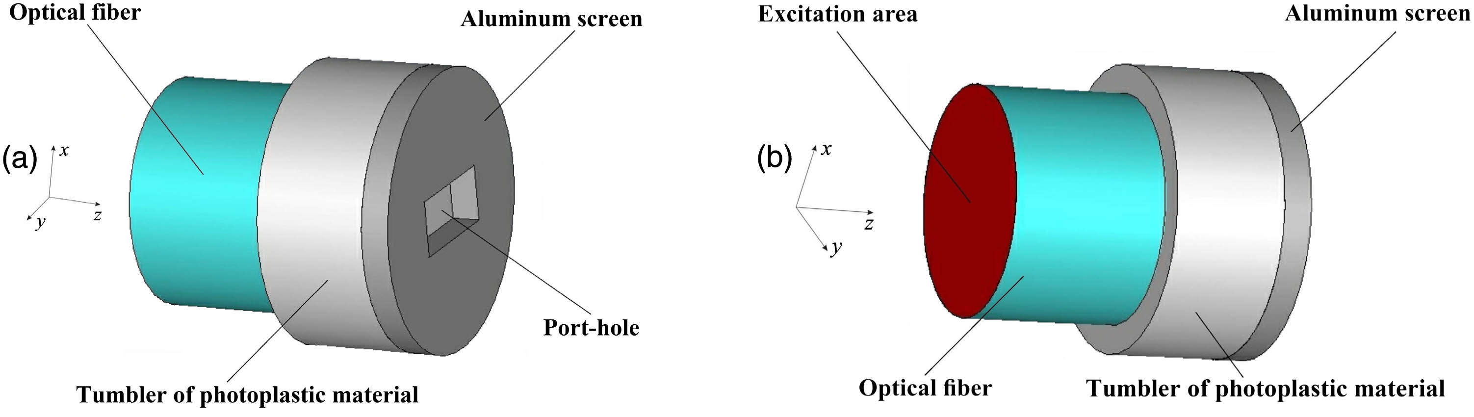
We propose a design for efficient end-fire coupling of surface plasmon polaritons in a metal-insulator-metal (MIM) waveguide with an optical fiber as part of a simple photoplastic connector. The design was analyzed and optimized using the three-dimensional finite-difference time-domain method. The calculated excitation efficiency coefficient of the waveguide is 83.7% ( 0.77 dB) at a wavelength of 405 nm. This design enables simple connection of an optical fiber to a MIM waveguide and highly efficient local excitation of the waveguide. Moreover, the length of the metallic elements of the waveguide, and thus the dissipative losses, can be reduced. The proposed design may be useful in plasmonic-type waveguide applications such as near-field investigation of live cells and other objects with super-resolution.
Buffers, couplers, routers, switches, and multipl Near-field microscopy Plasmonics Photonics Research
2018, 6(3): 03000149
Author Affiliations
Abstract
1 State Key Laboratory of Modern Optical Instrumentation, Zhejiang University, Hangzhou 310027, China
2 College of Science, Zhejiang University of Technology, Hangzhou 310028, China
We present compact silicon-arrayed waveguide grating routers (AWGRs) with three different channel spacings of 20, 6.4, and 3.2 nm for optical interconnect systems. The AWGR with the 20 nm channel spacing shows a low loss of 2.5 dB and a low crosstalk of 20 dB and has a footprint of only 0.27 mm×0.19 mm. The AWGR with the channel spacing of 6.4 nm has loss ranging from 3 to 8 dB, and the crosstalk is 18 dB. As for the 3.2 nm channel spacing, the loss is about 4 dB, and the crosstalk is 12 dB.
060.1810 Buffers, couplers, routers,switches, and multiplexers 130.3120 Integrated optics devices 200.4650 Optical interconnects Chinese Optics Letters
2017, 15(3): 030603
1 State Key Laboratory for Modern Optical Instrumentation, Centre for Optical and Electromagnetic Research,Zhejiang Provincial Key Laboratory for Sensing Technologies, Zhejiang University, Hangzhou 310058, China
2 Key Laboratory for Modern Optical Instrumentation, Centre for Optical and Electromagnetic Research,Zhejiang Provincial Key Laboratory for Sensing Technologies, Zhejiang University, Hangzhou 310058, China
Directional couplers (DCs) have been playing an important role as a basic element for realizing power exchange. Previously most work was focused on symmetric DCs and little work was reported for asymmetric directional couplers (ADCs). In recently years, silicon nanophotonic waveguides with ultra-high index contrast and ultra-small cross section have been developed very well and it has been shown that ADCs based on silicon-oninsulator (SOI) nanophotonic waveguides have some unique ability for polarization-selective coupling as well as mode-selective coupling, which are respectively very important for polarization-related systems and modedivision- mulitplexing systems. In this paper, a review is given for the recent progresses on silicon-based ADCs and the applications for power splitting, polarization beam splitting, as well as mode conversion/(de)multiplexing.
silicon photonics silicon photonics asymmetric directional couplers (ADCs) asymmetric directional couplers (ADCs) polarization-division multiplexing (PDM) polarization-division multiplexing (PDM) mode-division multiplexing (MDM) mode-division multiplexing (MDM) polarization beam splitter (PBSs) polarization beam splitter (PBSs) Frontiers of Optoelectronics
2016, 9(3): 450


