Photonics Research, 2020, 8 (7): 07001189, Published Online: Jun. 22, 2020  

All-optical PtSe2 silicon photonic modulator with ultra-high stability Download: 827次

Author Affiliations
1 Wuhan National Laboratory for Optoelectronics, Huazhong University of Science and Technology, Wuhan 430074, China
2 Institute of Microscale Optoelectronics, Collaborative Innovation Centre for Optoelectronic Science & Technology, Key Laboratory of Optoelectronic Devices and Systems of Ministry of Education and Guangdong Province, College of Physics and Optoelectronic Engineering, Shenzhen Key Laboratory of Micro-Nano Photonic Information Technology, Guangdong Laboratory of Artificial Intelligence and Digital Economy (SZ), Shenzhen University, Shenzhen 518060, China
3 e-mail: jjdong@mail.hust.edu.cn
4 e-mail: hzhang@szu.edu.cn
Abstract
All-optical modulation based on the photothermal effect of two-dimensional (2D) materials shows great promise for all-optical signal processing and communication. In this work, an all-optical modulator with a 2D PtSe2-on-silicon structure based on a microring resonator is proposed and demonstrated utilizing the photothermal effect of PtSe2. A tuning efficiency of 0.0040 nm · mW?1 is achieved, and the 10%–90% rise and decay times are 304 μs and 284 μs, respectively. The fabricated device exhibits a long-term air stability of more than 3 months. The experimental results prove that 2D PtSe2 has great potential for optical modulation on a silicon photonic platform.

1. INTRODUCTION

All-optical modulation has received extensive attention since it avoids the conversion of electrical signals to optical signals [1]. Although electrically driven modulators using such as charge carrier injecting effect [2], thermo-optic effect [3], and Pockels effect [4] have achieved great success on silicon and lithium niobate platforms, all-optical modulation still plays an irreplaceable role due to its simple structural design and easy manufacturing process. Meanwhile, novel two-dimensional (2D) materials emerging in recent years, such as graphene [5], black phosphorus (BP) [6], and transition metal dichalcogenides (TMDs) [7], provide more opportunities to implement all-optical signal processing, with respect to their distinct merits, such as intrinsic lattice matching with silicon, complementary metal oxide semiconductor integrability, as well as excellent electrical, optical, and thermal properties [8,9]. Li et al. demonstrate all-optical intensity modulation in a graphene-clad microfiber by using Pauli blocking in graphene; an ultra-fast decay time of 2.2 ps and a modulation depth of 38% are achieved [5]. Thermo-optic effect [10] is also used to achieve all-optical phase modulation in the microfiber assisted by graphene [11], BP [6], MXene [12], or tungsten disulfide (WS2) [7], but the response time is of the order of milliseconds. The integrated photonic platform offers higher compactness and potential for manufacturing large-scale photonic integrated circuits [13,14]. All-optical modulation based on an integrated platform has been intensively studied using photo-excited free-carrier concentrations [15], electromagnetic induced transparency [16], reverse saturable absorption [17], or photothermal effect (assisted by metal–insulator–metal absorbers) [1820" target="_self" style="display: inline;">–20], etc. However, 2D material-based all-optical modulation on an integrated photonic platform has been rarely reported [2124" target="_self" style="display: inline;">24]. It is essential to explore the potential of 2D materials to achieve all-optical modulation on an integrated photonic platform.

As a group of representative 2D materials, TMDs are composed of two chalcogen (X) atomic layers and a transition metal (M) atomic layer sandwiched between them [25]. Compared with the zero bandgap and weak optical absorption (2.3%) of monolayer graphene [26], TMDs have bandgaps that change with the number of layers and strong resonant absorption at specific wavelengths [27]. In addition, TMDs can be prepared by the chemical vapor deposition (CVD) method and other bottom-up growth techniques, which reveal the advantages of excellent uniformity, controllable number of layers, strong reliability, high repeatability, and large area preparation [28,29].

Platinum selenide (PtSe2), a new type of layered TMD, has been intensively studied due to its special properties since it was first epitaxially grown by direct selenization of Pt on a substrate [30]. Its crystal structure can be regarded as being composed of hexagonal closely arranged Se atoms with Pt atoms occupying octahedral sites in alternate Se layers [25]. Different from other TMDs with large bandgaps (such as monolayer MoS2:1.78  eV) [31,32], monolayer PtSe2 has a smaller indirect bandgap of 1.2 eV, while the bilayer directly reduces to 0.21 eV [25,33]. If the thickness continues to increase, it will eventually become a Type II Dirac semimetal without a bandgap [30,3436" target="_self" style="display: inline;">–36], and the absorption of light in a specific band (especially in the range of less than 1000 nm) is even higher than that of an Au film [37]. Previous works have applied 2D PtSe2 to a saturation absorber, photodetector, and field effect transistor, and confirmed that wideband responses can be achieved by changing the number of layers [25,3745" target="_self" style="display: inline;">45]. In addition, PtSe2 is predicted to have the highest carrier mobility of 4000  cm2·V1·s1 at room temperature among reported TMDs [46], and a long-term air stability for over 1 year has been reported [47].

In this work, we propose and experimentally demonstrate an all-optical modulator with a 2D PtSe2-on-silicon structure. The PtSe2 material is grown with the CVD method and then transferred onto a silicon microring resonator (MRR). By using a 980 nm laser to irradiate the surface of the device from free space, we successfully demonstrate all-optical modulation based on the photothermal conversion of PtSe2. A tuning efficiency of 0.0040  nm·mW1 is achieved. The dynamic 10%–90% rise/decay time is 304/284 μs, and the 3 dB bandwidth is measured to be 2.4 kHz. We also perform a comparative experiment on a pure silicon device and confirm that the photothermal conversion efficiency almost entirely comes from the 2D PtSe2. Due to the outstanding air stability of PtSe2, the tuning efficiency of the fabricated device only decreased by 7.5% after being exposed to the air for 3 months, which exhibits the long-term stability of this all-optical modulator. Results show that the PtSe2-based device is a potential option to be deployed in all-optical signal processing, showing great advantages in low cost and easy fabrication.

2. DEVICE FABRICATION AND PRINCIPLE

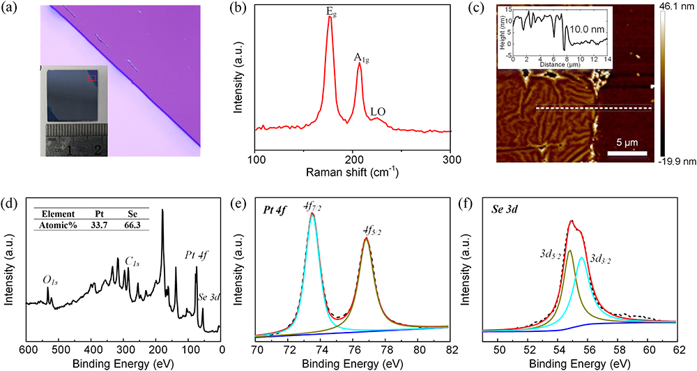
The optical microscopy image of the as-prepared PtSe2 film is illustrated in Fig. 1(a), which indicates that the film is uniform in large size. As shown in Fig. 1(b), three pronounced Raman peaks can be found at 176.2  cm1, 207.1  cm1, and 225.2  cm1, corresponding to the Eg, A1g, and LO vibrational modes of Se atoms, respectively. The positions of these Raman peaks are well consistent with the previously reported values [48,49], which confirms the quality of the as-grown PtSe2 film. The thickness and surface topography of the transferred PtSe2 are characterized by an atomic force microscope (AFM). As shown in Fig. 1(c), the film thickness is determined to be 10.0 nm. However, there are many folds as transferred to the surface of the chip, so the actual thickness of PtSe2 film will be slightly smaller, and the number of layers is about 13 [33]. The species and chemical states of the elements in the PtSe2 film are analyzed by X-ray photoelectron spectroscopy (XPS). According to the XPS analysis, the film has predominant C, O, Pt, and Se peaks shown in Fig. 1(d). However, the peaks of C1s and O1s originate from the absorbed air in the surface of the PtSe2 film. As shown in Figs. 1(e) and 1(f), the Pt 4f and Se 3d spectra of PtSe2 are fitted considering two peaks by Gaussian fitting. According to the fitting spectra, there are two peaks at 73.52 eV and 76.83 eV that are related to Pt 4f7/2 and Pt 4f5/2 orbitals, respectively. Moreover, the peaks located at 54.81 eV and 55.59 eV are related to Se 3d5/2 and Se 3d3/2. The atomic ratios of Pt and Se calculated on the basis of XPS spectra are shown in the inset of Fig. 1(d), which is quite consistent with the theoretical value.

Fig. 1. (a) Optical microscopy image of the CVD grown PtSe2 film. (b) Raman spectrum of PtSe2 film. (c) AFM image of the transferred PtSe2 and the typical height profile along the white dashed line. XPS spectra of (d) the PtSe2 film, (e) the Pt 4f region, and (f) the Se 3d region.

下载图片 查看所有图片

The microscope images of the all-optical MRR modulator are displayed in Figs. 2(a) and 2(b). Our device is fabricated on a silicon-on-insulator (SOI) wafer with a 220 nm thick silicon layer and a 2 μm thick SiO2 buried oxide layer, using standard electron beam lithography followed by the inductively couple plasma etching process. The device consists of a ring-shaped waveguide and a side coupled straight waveguide, where the radius of the ring is 50 μm and the gap of the coupling region is 80 nm. The width of the waveguide is 550 nm and the height is 220 nm. There is a pair of tapered grating couplers at both ends of the straight waveguide for optical coupling between the fiber and the chip. A 10 nm thick Al2O3 isolation layer is deposited onto the SOI wafer using the atomic layer deposition method, as shown in Fig. 2(c). Finally, the PtSe2 thin film is transferred to the device surface by the wet-transfer process.

Fig. 2. (a) Microscope image of the all-optical modulator where PtSe2 film fully covers the whole device. (b) A zoom-in on the part of the MRR shows uniformly transferred thin film. (c) Cross section of the PtSe2-on-silicon structure. (d) Transmission spectra of the MRR without (brown) and with (blue) the PtSe2 film (normalized respectively). (e) All-optical modulation mechanism and experimental setup of the PtSe2-based modulator. TLS, tunable laser source; ASE, amplified spontaneous emission; PC, polarization controller; SMF, single-mode fiber; OSA, optical spectrum analyzer; PD, photodetector; OSCP, oscilloscope.

下载图片 查看所有图片

Figure 2(d) shows the transmission spectra of the MRR with and without 2D PtSe2 film. The MRR initially operates at the over coupling condition with an extinction ratio (ER) of 3–4 dB and a free spectral range (FSR) of 1.8  nm. As the waveguide is coated by PtSe2 film, the round-trip loss of the MRR increases due to the light absorption and the edge scattering effect, while the coupling coefficient between the straight waveguide and the ring may also have changed [50]. Thus, the device works closer to the critical coupling condition with an ER of 5–6 dB. Moreover, the effective refractive index of the grating couplers changes and the peak wavelength moves to a longer wavelength once they were covered by the 2D PtSe2 film. In fact, the extra loss caused by the transferred material is 16  dB by comparing the transmittance before and after transferring material, including the optical absorption of the material and the deterioration on the grating couplers.

The resonance wavelength of the MRR is given by Eq. (1): where neff is the effective refractive index of the PtSe2/Al2O3/silicon hybrid waveguide at a specific wavelength, r isthe radius of the MRR, and m is the resonance order of corresponding wavelength λm. As shown in Fig. 2(e), the PtSe2 film will absorb the pump light and heat the waveguide underneath due to the photothermal effect. The increase in temperature causes the effective refractive index to change, which performs a redshift in the output spectrum. When the probe light (signal light) of a specific wavelength is injected into the waveguide, the output optical power is t1 (in dB). After being heated by the pump light, the corresponding output power changes to t2 (in dB). Therefore, the output light intensity is modulated by the pump light with a modulation depth (MD) of Δt=|t1t2|.

3. EXPERIMENTAL SETUP

The experimental setup of the proposed all-optical modulator is schematically shown in Fig. 2(e). An amplified spontaneous emission (ASE, ALS-18-B-FA, Amonics) light and a tunable laser source (TLS) as a probe light are combined by a 3 dB fiber coupler and then injected into the chip through a single-mode fiber (SMF) and a grating coupler. The polarization of the light beam is controlled by the polarization controller to obtain the quasi-transverse electric mode transmitting in the designed waveguide, which limits the optical field of the probe light to the center of the waveguide to reduce optical loss. Then the output light is coupled into the SMF by another identical grating coupler. Pump light [produced by a home-made programmable 980 nm laser source, which can work in the continuous-wave (CW) mode or square-wave (SW) mode] directly irradiates the device surface through an SMF. Only ASE is turned on at the input end when the pump laser works in the CW mode, and the output SMF is connected to an optical spectrum analyzer (AQ6370D, Yokogawa) to monitor the transmission spectrum of the MRR. Only the TLS is turned on when the pump laser works in the SW mode, and the output SMF switches to the photodetector (DET08CFC/M InGaAs Biased Detector, Thorlabs) and oscilloscope (MDO4104C, Tektronix) path to obtain the dynamic modulation response. All the experiments were carried out at room temperature.

4. RESULTS AND DISCUSSION

4.1 A. Experimental Results

The static pump results are shown in Fig. 3. The FSR of the MRR is given by Eq. (2): where λ is the center wavelength, and ng is the group index of the waveguide. In order to obtain the maximum MD, the spectral shift produced by the pump light should be larger than half of the full width of the resonance peak. However, the Q value of the device decreases after the PtSe2 film is transferred, as shown in Fig. 2(d), so the spectral shift must be larger than half of the FSR.

Fig. 3. (a) Static spectral response for different pump powers. (b) Measured resonance shift versus pump power and the corresponding linear fitting curves, for pristine PtSe2 device (red) and the device after 3-month air exposure (blue).

下载图片 查看所有图片

The pump power from 0 to 210.9 mW (measured by a hand-held power meter, FPM-300 Power Meter, EXFO) is applied to measure the static response of the device when a 980 nm laser source works in the CW mode. The results in Fig. 3(a) indicate that a phase modulation is obtained in the PtSe2-based modulator. Once the pump power is reduced, the spectrum will move back to its initial position. The maximum spectral shift is 0.962 nm (i.e., 1.069π), and the calculated tuning efficiency is 0.0040  nm·mW1 or 0.0044πmW1 [red line in Fig. 3(b)]. Compared to the pure silicon device with a tuning efficiency of 0.00047  nm·mW1 or 0.00023πmW1 (see static spectral response of the pure silicon device in Appendix A), the heating efficiency improvement mainly comes from the PtSe2 film. In order to investigate the stability of the modulator, the static response of the device was tested again after 3 months of exposure to air. As shown in Fig. 3(b) (blue line), a spectral shift of 1.156 nm (i.e., 1.284π) is obtained when the maximum pump power is set to be 300 mW, and the tuning efficiency is 0.0037  nm·mW1, which is almost maintained the same as that of the newly fabricated device. These results prove that the all-optical modulator based on 2D PtSe2 has a long-term air stability.

To characterize the dynamic response of the device, the 980 nm pump laser operates in the 100 Hz SW mode with a power of 210 mW [Fig. 4(a)], and the wavelength of the TLS is selected as 1550.3 nm. The corresponding probe light waveform is shown in Fig. 4(b), and the 10%–90% rise and decay times are measured to be 304 μs and 284 μs, respectively. This is 1 order of magnitude faster than that of graphene- and BP-based all-optical modulators using the photothermal effect with a microfiber structure [6,11]. The frequency response of the modulator is further studied by a faster SW signal with the frequency varying from 200 Hz to 10 kHz. Several measured waveforms of the modulated probe light with different frequencies are shown in Fig. 4(c). As the frequency increases, the modulated signal waveform gradually deforms from square wave to triangle wave, and the peak-to-peak voltage (Vpp) of the signal keeps decreasing as the frequency increases, which is mainly attributed to the hysteresis effect of slow heat generation and dissipation [6]. The tendency of Vpp versus modulation frequency is shown in Fig. 4(d), and the fitted 3 dB bandwidth of the device is 2.4 kHz, which is close to the measured rise/decay time.

Fig. 4. (a) Pump light with 100 Hz frequency and (b) the corresponding modulated signal light. (c) Several signal waveforms at different frequencies. (d) Vpp versus modulation frequency.

下载图片 查看所有图片

4.2 B. Discussions

In order to evaluate the true photothermal efficiency of the PtSe2, the photothermal conversion efficiency of the modulator is calculated by combining the thermo-optic and thermal expansion theory of silicon with Eq. (1). With the increase of temperature, the effective refractive index and length of the waveguide in the region of the pump light irradiation (spot size L80  μm) will change because of the thermo-optic and thermal expansion effects of silicon [51], as shown in Eqs. (3) and (4): where C=1.8×10⁴  K1 is the thermo-optic coefficient [52] and α=2.63×10⁶  K1 is the thermal expansion coefficient [51] of silicon, and T0 is the temperature before heating. For an MRR, the spectral shift of the m-order resonant wavelength after heating can be obtained by substituting Eqs. (3) and (4) into Eq. (1): It can be calculated that the desired temperature change to obtain 1 nm resonance shift around 1550 nm is ΔT13.9  K according to Eq. (5), and the refractive index change of the specific waveguide region is Δn2.5×103. In fact, the thermal expansion coefficient is 2 orders of magnitude smaller than the thermo-optic coefficient, and its effect is almost negligible. As shown in Fig. 3(b), the pump power corresponding to a spectral shift of 1 nm in the static test is 250  mW. An infrared thermal camera is used to characterize the surface temperature change of the fabricated modulator under different pump power in real time, as shown in Figs. 5(a) and 5(b). The maximum pump power is up to 500 mW in test, and the surface temperature change is ΔT=1.827  K with a fitted temperature-power coefficient of 0.0036 K · mW−1, as shown in Fig. 5(c). Therefore, when the 250 mW pump light heats the device, it will cause a temperature change of ΔT=0.9  K. This is smaller than our theoretical value, and the reason lies in that the 980 nm pulsed laser is used in the surface temperature test. Its pump energy is lower than that of the CW laser, and the SMF moves far from the modulator due to the restraints of test equipment, thus resulting in a larger light spot and less energy per unit area. At the same time, the heat is more likely to diffuse to areas outside the MRR.

Fig. 5. Infrared thermograms of the PtSe2 modulator with pump powers of (a) 50 mW and (b) 500 mW. (c) Surface temperature change of the modulator versus pump power.

下载图片 查看所有图片

Fig. 6. (a) Optical microscopy image of the pure silicon MZI. (b) Static spectral response for different pump powers. (c) Measured resonance shift versus pump power and the corresponding fitting curve.

下载图片 查看所有图片

Here a comparison of the reported all-optical modulators based on the photothermal effect of 2D materials is summarized in Table 1. The on-chip waveguide modulators obviously have better compactness and faster modulation speed compared with the modulators using the microfiber structure. In addition, compared with the weak light absorption of graphene on Si3N4 waveguide [22], the greater light absorption of PtSe2 means a lower pump power consumption can be achieved theoretically. Although both schemes achieve the same level of tuning efficiency with interaction lengths <100  μm, considering that when the pump light is irradiated from free space, the width of the waveguide (550 nm) is much smaller than the diameter of the light spot (80  μm). This means that more than 80% of the energy in the spot cannot be used to effectively heat the microring waveguide (assuming that the energy distribution of the pump spot is similar to the fundamental mode in the SMF). It can be expected that the PtSe2-based device can achieve better tuning efficiency with optimized pumping methods.

Table 1. Comparison of Reported All-Optical Modulators Based on the Photothermal Effect of 2D Materials

Pump WavelengthProbe WavelengthInteraction LengthSwitching TimeTuning Efficiency
MaterialStructure(nm)(nm)(μm)(μs)(nm·mW1)Refs.
BPSilica fiber980155025000.0043[6]
WS2Silica fiber980155050073000.0015[7]
MXeneSilica fiber980155050041000.0086[12]
AntimoneneSilica fiber98015505029000.0162[53]
GrapheneSilica fiber980/15401550500032000.0045[11]
GrapheneSi3N4 waveguide1555150943.40.2530.0079[22]
PtSe2Silicon waveguide9801550802840.0040This work

查看所有表

Therefore, it is possible to achieve more efficient pumping by using a lensed fiber tip to reduce the size of the spot [20]. The silicon-based thermo-optic modulator has achieved a response time of 0.6 μs [3], which means accurate material etching and specific optimized air gaps that can help the heat distribution to be concentrated on the waveguide rather than spread far away [20], which may further improve the modulation efficiency and response speed of the device. In addition, the demanded spectral shift and the corresponding pump power can be reduced by optimizing the Q factor of the device. The optical losses of the device are mainly attributed to the contamination during the process of material transferring and the absorption caused by the material covering the grating couplers and other non-pumping parts, which can be eliminated by patterning definition [54].

5. CONCLUSION

In conclusion, we propose and demonstrate an all-optical modulator with a PtSe2-on-silicon structure. By utilizing the photothermal effect of PtSe2, we successfully convert the information from pump light to probe light. The device achieves a modulation bandwidth of 2.4 kHz with a 10%–90% rise/decay time of 304/284 μs, and the tuning efficiency is 0.0040  nm·mW1. Thanks to the long-term stability of PtSe2 in the air, the tuning efficiency of the device keeps almost unchanged after 3 months. This work brings 2D PtSe2 to the field of silicon-based photothermal modulation devices for the first time and shows its great potential for the all-optical information processing field, such as optical routing, switching, and logic gate and sensing, with low cost and simple manufacturing process.

6 Acknowledgment

Acknowledgment. The authors also acknowledge the support from Instrumental Analysis Center of Shenzhen University (Xili Campus).

References

[1] P. Minzioni, C. Lacava, T. Tanabe, J. Dong, X. Hu, G. Csaba, W. Porod, G. Singh, A. E. Willner, A. Almaiman. Roadmap on all-optical processing. J. Opt., 2019, 21: 063001.

[2] Q. Xu, B. Schmidt, S. Pradhan, M. Lipson. Micrometre-scale silicon electro-optic modulator. Nature, 2005, 435: 325-327.

[3] X. Wang, A. Lentine, C. DeRose, A. L. Starbuck, D. Trotter, A. Pomerene, S. Mookherjea. Wide-range and fast thermally-tunable silicon photonic microring resonators using the junction field effect. Opt. Express, 2016, 24: 23081-23093.

[4] M. He, M. Xu, Y. Ren, J. Jian, Z. Ruan, Y. Xu, S. Gao, S. Sun, X. Wen, L. Zhou, L. Liu, C. Guo, H. Chen, S. Yu, L. Liu, X. Cai. High-performance hybrid silicon and lithium niobate Mach-Zehnder modulators for 100 Gbit s-1 and beyond. Nat. Photonics, 2019, 13: 359-364.

[5] W. Li, B. Chen, C. Meng, W. Fang, Y. Xiao, X. Li, Z. Hu, Y. Xu, L. Tong, H. Wang. Ultrafast all-optical graphene modulator. Nano Lett., 2014, 14: 955-959.

[6] Y. Wang, F. Zhang, X. Tang, X. Chen, Y. Chen, W. Huang, Z. Liang, L. Wu, Y. Ge, Y. Song. All‐optical phosphorene phase modulator with enhanced stability under ambient conditions. Laser Photonics Rev., 2018, 12: 1800016.

[7] K. Wu, C. Guo, H. Wang, X. Zhang, J. Wang, J. Chen. All-optical phase shifter and switch near 1550  nm using tungsten disulfide (WS2) deposited tapered fiber. Opt. Express, 2017, 25: 17639-17649.

[8] F. Koppens, T. Mueller, P. Avouris, A. Ferrari, M. Vitiello, M. Polini. Photodetectors based on graphene, other two-dimensional materials and hybrid systems. Nat. Nanotechnol., 2014, 9: 780-793.

[9] F. Xia, H. Wang, D. Xiao, M. Dubey, A. Ramasubramaniam. Two-dimensional material nanophotonics. Nat. Photonics, 2014, 8: 899-907.

[10] K. Wu, Y. Wang, C. Qiu, J. Chen. Thermo-optic all-optical devices based on two-dimensional materials. Photon. Res., 2018, 6: C22-C28.

[11] X. Gan, C. Zhao, Y. Wang, D. Mao, L. Fang, L. Han, J. Zhao. Graphene-assisted all-fiber phase shifter and switching. Optica, 2015, 2: 468-471.

[12] Q. Wu, S. Chen, Y. Wang, L. Wu, X. Jiang, F. Zhang, X. Jin, Q. Jiang, Z. Zheng, J. Li, M. Zhang, H. Zhang. MZI-based all-optical modulator using MXene Ti3C2Tx (T = F, O, or OH) deposited microfiber. Adv. Mater. Technol., 2019, 4: 1800532.

[13] J. S. Fandiño, P. Muñoz, D. Doménech, J. Capmany. A monolithic integrated photonic microwave filter. Nat. Photonics, 2017, 11: 124-129.

[14] D. Marpaung, J. Yao, J. Capmany. Integrated microwave photonics. Nat. Photonics, 2019, 13: 80-90.

[15] V. R. Almeida, C. A. Barrios, R. R. Panepucci, M. Lipson. All-optical control of light on a silicon chip. Nature, 2004, 431: 1081-1084.

[16] M. Miscuglio, A. Mehrabian, Z. Hu, S. I. Azzam, J. George, A. V. Kildishev, M. Pelton, V. J. Sorger. All-optical nonlinear activation function for photonic neural networks [Invited]. Opt. Mater. Express, 2018, 8: 3851-3863.

[17] S. I. Azzam, A. V. Kildishev. Time-domain dynamics of reverse saturable absorbers with application to plasmon-enhanced optical limiters. Nanophotonics, 2018, 8: 145-151.

[18] X. Chen, Y. Chen, Y. Shi, M. Yan, M. Qiu. Photothermal switching of SOI waveguide-based Mach-Zehnder interferometer with integrated plasmonic nanoheater. Plasmonics, 2014, 9: 1197-1205.

[19] X. Chen, Y. Shi, F. Lou, Y. Chen, M. Yan, L. Wosinski, M. Qiu. Photothermally tunable silicon-microring-based optical add-drop filter through integrated light absorber. Opt. Express, 2014, 22: 25233-25241.

[20] H. Gong, X. Chen, Y. Qu, Q. Li, M. Yan, M. Qiu. Photothermal switching based on silicon Mach-Zehnder interferometer integrated with light absorber. IEEE Photonics J., 2016, 8: 7802610.

[21] Z. Shi, L. Gan, T.-H. Xiao, H.-L. Guo, Z.-Y. Li. All-optical modulation of a graphene-cladded silicon photonic crystal cavity. ACS Photonics, 2015, 2: 1513-1518.

[22] C. Qiu, Y. Yang, C. Li, Y. Wang, K. Wu, J. Chen. All-optical control of light on a graphene-on-silicon nitride chip using thermo-optic effect. Sci. Rep., 2017, 7: 17046.

[23] M. Ono, M. Hata, M. Tsunekawa, K. Nozaki, H. Sumikura, H. Chiba, M. Notomi. Ultrafast and energy-efficient all-optical switching with graphene-loaded deep-subwavelength plasmonic waveguides. Nat. Photonics, 2020, 14: 37-43.

[24] H. Wang, N. Yang, L. Chang, C. Zhou, S. Li, M. Deng, Z. Li, Q. Liu, C. Zhang, Z. Li, Y. Wang. CMOS-compatible all-optical modulator based on the saturable absorption of graphene. Photon. Res., 2020, 8: 468-474.

[25] B. Yan, B. Zhang, H. Nie, G. Li, J. Liu, B. Shi, K. Yang, J. He. Bilayer platinum diselenide saturable absorber for 2.0 μm passively Q-switched bulk lasers. Opt. Express, 2018, 26: 31657-31663.

[26] R. R. Nair, P. Blake, A. N. Grigorenko, K. S. Novoselov, T. J. Booth, T. Stauber, N. M. Peres, A. K. Geim. Fine structure constant defines visual transparency of graphene. Science, 2008, 320: 1308.

[27] K. F. Mak, J. Shan. Photonics and optoelectronics of 2D semiconductor transition metal dichalcogenides. Nat. Photonics, 2016, 10: 216-226.

[28] B. Guo. 2D noncarbon materials-based nonlinear optical devices for ultrafast photonics. Chin. Opt. Lett., 2018, 16: 020004.

[29] A. Krasnok, S. Lepeshov, A. Alú. Nanophotonics with 2D transition metal dichalcogenides [Invited]. Opt. Express, 2018, 26: 15972-15994.

[30] Y. Wang, L. Li, W. Yao, S. Song, J. T. Sun, J. Pan, X. Ren, C. Li, E. Okunishi, Y.-Q. Wang, E. Wang, Y. Shao, Y. Y. Zhang, H.-T. Yang, E. F. Schwier, H. Iwasawa, K. Shimada, M. Taniguchi, Z. Cheng, S. Zhou, S. Du, S. J. Pennycook, S. T. Pantelides, H.-J. Gao. Monolayer PtSe2, a new semiconducting transition-metal-dichalcogenide, epitaxially grown by direct selenization of Pt. Nano Lett., 2015, 15: 4013-4018.

[31] H.-P. Komsa, A. V. Krasheninnikov. Electronic structures and optical properties of realistic transition metal dichalcogenide heterostructures from first principles. Phys. Rev. B, 2013, 88: 085318.

[32] W. Zhao, R. M. Ribeiro, M. Toh, A. Carvalho, C. Kloc, A. H. Castro Neto, G. Eda. Origin of indirect optical transitions in few-layer MoS2, WS2, and WSe2. Nano Lett., 2013, 13: 5627-5634.

[33] Z. Wang, Q. Li, F. Besenbacher, M. Dong. Facile synthesis of single crystal PtSe2 nanosheets for nanoscale electronics. Adv. Mater., 2016, 28: 10224-10229.

[34] H. Huang, S. Zhou, W. Duan. Type-II Dirac fermions in the PtSe2 class of transition metal dichalcogenides. Phys. Rev. B, 2016, 94: 121117.

[35] K. Zhang, M. Yan, H. Zhang, H. Huang, M. Arita, Z. Sun, W. Duan, Y. Wu, S. Zhou. Experimental evidence for type-II Dirac semimetal in PtSe2. Phys. Rev. B, 2017, 96: 125102.

[36] H. Yang, M. Schmidt, V. Süss, M. Chan, F. F. Balakirev, R. D. McDonald, S. S. P. Parkin, C. Felser, B. Yan, P. J. W. Moll. Quantum oscillations in the type-II Dirac semi-metal candidate PtSe2. New J. Phys., 2018, 20: 043008.

[37] J. Xie, D. Zhang, X.-Q. Yan, M. Ren, X. Zhao, F. Liu, R. Sun, X. Li, Z. Li, S. Chen. Optical properties of chemical vapor deposition-grown PtSe2 characterized by spectroscopic ellipsometry. 2D Mater., 2019, 6: 035011.

[38] C. Yim, K. Lee, N. McEvoy, M. O’Brien, S. Riazimehr, N. C. Berner, C. P. Cullen, J. Kotakoski, J. C. Meyer, M. C. Lemme, G. S. Duesberg. High-performance hybrid electronic devices from layered PtSe2 films grown at low temperature. ACS Nano, 2016, 10: 9550-9558.

[39] C. Yim, N. McEvoy, S. Riazimehr, D. S. Schneider, F. Gity, S. Monaghan, P. K. Hurley, M. C. Lemme, G. S. Duesberg. Wide spectral photoresponse of layered platinum diselenide-based photodiodes. Nano Lett., 2018, 18: 1794-1800.

[40] J. Yuan, H. Mu, L. Li, Y. Chen, W. Yu, K. Zhang, B. Sun, S. Lin, S. Li, Q. Bao. Few-layer platinum diselenide as a new saturable absorber for ultrafast fiber lasers. ACS Appl. Mater. Interfaces, 2018, 10: 21534-21540.

[41] D. Wu, Y. Wang, L. Zeng, C. Jia, E. Wu, T. Xu, Z. Shi, Y. Tian, X. Li, Y. H. Tsang. Design of 2D layered PtSe2 heterojunction for the high-performance, room-temperature, broadband, infrared photodetector. ACS Photonics, 2018, 5: 3820-3827.

[42] L. Zeng, S. Lin, Z. Lou, H. Yuan, H. Long, Y. Li, W. Lu, S. P. Lau, D. Wu, Y. H. Tsang. Ultrafast and sensitive photodetector based on a PtSe2/silicon nanowire array heterojunction with a multiband spectral response from 200 to 1550  nm. NPG Asia Mater., 2018, 10: 352-362.

[43] L.-H. Zeng, S.-H. Lin, Z.-J. Li, Z.-X. Zhang, T.-F. Zhang, C. Xie, C.-H. Mak, Y. Chai, S. P. Lau, L.-B. Luo, Y. H. Tsang. Fast, self-driven, air-stable, and broadband photodetector based on vertically aligned PtSe2/GaAs heterojunction. Adv. Functional Mater., 2018, 28: 1705970.

[44] R. Zhuo, L. Zeng, H. Yuan, D. Wu, Y. Wang, Z. Shi, T. Xu, Y. Tian, X. Li, Y. H. Tsang. In-situ fabrication of PtSe2/GaN heterojunction for self-powered deep ultraviolet photodetector with ultrahigh current on/off ratio and detectivity. Nano Res., 2019, 12: 183-189.

[45] K. Zhang, M. Feng, Y. Ren, F. Liu, X. Chen, J. Yang, X. Yan, F. Song, J. Tian. Q-switched and mode-locked Er-doped fiber laser using PtSe2 as a saturable absorber. Photon. Res., 2018, 6: 893-899.

[46] Z. Huang, X. Yu, W. Zhang, P. Yu, D. Wu, W. Zhang, B. Singh, Q. Zeng, H. Lin, W. Zhou, J. Lin, K. Suenaga, Z. Liu. Atomically thin noble metal dichalcogenide: a broadband mid-infrared semiconductor. Nat. Commun., 2018, 9: 1545.

    . Computational search for two-dimensional MX2 semiconductors with possible high electron mobility at room temperature. Materials, 2016, 9: 716.

[47] Y. Zhao, J. Qiao, Z. Yu, P. Yu, K. Xu, S. P. Lau, W. Zhou, Z. Liu, X. Wang, W. Ji, Y. Chai. High-electron-mobility and air-stable 2D layered PtSe2 FETs. Adv. Mater., 2017, 29: 1604230.

[48] M. O’Brien, N. McEvoy, C. Motta, J.-Y. Zheng, N. C. Berner, J. Kotakoski, K. Elibol, T. J. Pennycook, J. C. Meyer, C. Yim, M. Abid, T. Hallam, J. F. Donegan, S. Sanvito, G. S. Duesberg. Raman characterization of platinum diselenide thin films. 2D Mater., 2016, 3: 021004.

[50] M. H. Tahersima, Z. Ma, Y. Gui, S. Sun, H. Wang, R. Amin, H. Dalir, R. Chen, M. Miscuglio, V. J. Sorger. Coupling-enhanced dual ITO layer electro-absorption modulator in silicon photonics. Nanophotonics, 2019, 8: 1559.

[51] L. Xin, W. Luna, G. Shiliang, L. Zhiquan, Y. Ming. Doubled temperature measurement range for a single micro-ring sensor. Acta Phys. Sinica, 2014, 63: 154209.

[52] R. Espinola, M. Tsai, J. T. Yardley, R. Osgood. Fast and low-power thermooptic switch on thin silicon-on-insulator. IEEE Photonics Technol. Lett., 2003, 15: 1366-1368.

[53] Y. Wang, W. Huang, C. Wang, J. Guo, F. Zhang, Y. Song, Y. Ge, L. Wu, J. Liu, J. Li, H. Zhang. An all-optical, actively Q-switched fiber laser by an antimonene-based optical modulator. Laser Photonics Rev., 2019, 13: 1800313.

[54] S. Yan, X. Zhu, L. H. Frandsen, S. Xiao, N. A. Mortensen, J. Dong, Y. Ding. Slow-light-enhanced energy efficiency for graphene microheaters on silicon photonic crystal waveguides. Nat. Commun., 2017, 8: 14411.

Kangkang Wei, Delong Li, Zhitao Lin, Zhao Cheng, Yuhan Yao, Jia Guo, Yunzheng Wang, Yupeng Zhang, Jianji Dong, Han Zhang, Xinliang Zhang. All-optical PtSe2 silicon photonic modulator with ultra-high stability[J]. Photonics Research, 2020, 8(7): 07001189.


引用该论文: TXT   |   EndNote

相关论文

加载中...

关于本站 Cookie 的使用提示

中国光学期刊网使用基于 cookie 的技术来更好地为您提供各项服务,点击此处了解我们的隐私策略。 如您需继续使用本网站,请您授权我们使用本地 cookie 来保存部分信息。
全站搜索
您最值得信赖的光电行业旗舰网络服务平台!