Photonics Research, 2018, 6 (7): 07000734, Published Online: Jul. 4, 2018
Surface-illuminated photon-trapping high-speed Ge-on-Si photodiodes with improved efficiency up to 1700 nm
Figures & Tables
Fig. 1. Schematics of Ge/Si PD active layers (a) without holes and (b) with photon-trapping holes. The Ge-on-Si PD is composed of 0.2 μm p+Ge (blue), 2 μm i-Ge (green), and 0.2 μm n+Si (silver) layers. The yellow rings are the Al/Ti/Pt ohmic contacts. The red circle with the “−” sign and the dark circle with the “+” sign represent photon-generated electron and hole, respectively.
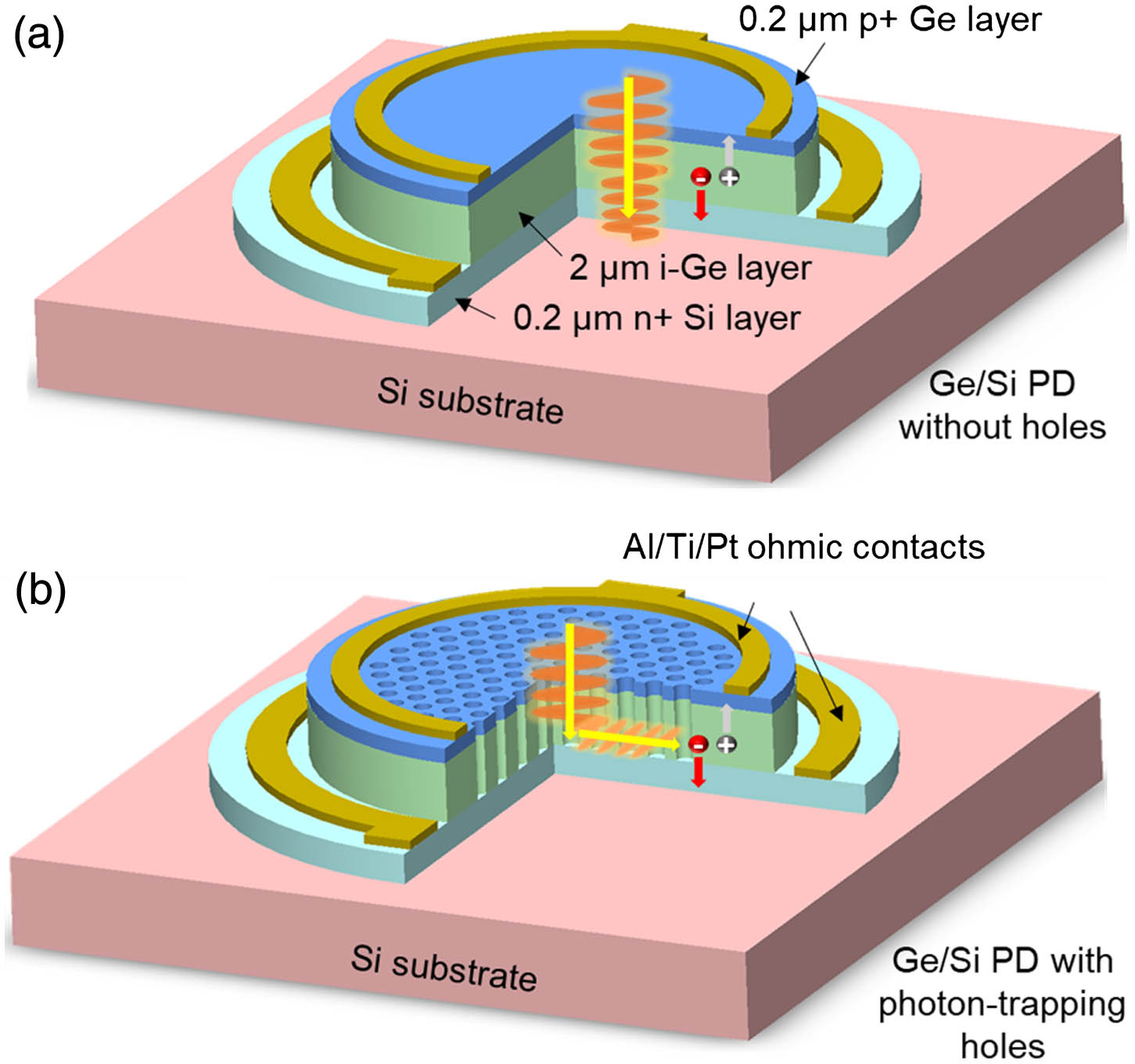
Fig. 2. (a) Schematic diagram that shows the enhanced optical path in a slab with hole arrays by light guiding near-perpendicular to the incoming light compared to an optical path in a bulk semiconductor in the direction of incident light. The effective absorption coefficient of a slab with hole arrays becomes much larger than the bulk absorption coefficient of the semiconductor due to the enhanced optical path. A thin slab with hole arrays can be used in a fast photodiode without losing efficiency, whereas a thick bulk semiconductor causes the photodiode to operate at slow speed in order to work efficiently. Typical field distributions around microholes at (b) t = 6 fs t = 15 fs t = 27 fs t = 48 fs 4.B ). The top and bottom rows show cross sections and top views of the electric field. The border of a hole with a taper at the top is represented by white lines. (f) Simulated electric field intensity of light at 1550 nm wavelength, propagating from air into a Ge-on-Si slab without hole arrays at t = 48 fs

Fig. 3. (a) Calculated absorption of Ge-on-Si PDs with (red line) and without (black line) tapered holes (diameter/period: 1150/1750 nm) arranged in a hexagonal lattice for a wavelength range of 1200–1800 nm. A 0.2% strain in the Ge layer is considered during calculations. The simulated structures have a 2 μm i-layer as shown in Fig. 1 . While Ge-on-Si PDs without holes theoretically absorb until 1550 nm, PDs with holes potentially keep high absorption of light up to 1700 nm. The green and blue lines represent absorption of PDs with and without holes, respectively, in the case of relaxed Ge layer as a comparison. 0.2% strain does not cause a significant difference for PDs with holes, whereas there is some improvement in absorption of PDs without holes toward longer wavelengths when a 0.2% strain is introduced to the Ge layer. (b) The calculated transmission and reflection (inset) for PDs with (red lines) and without (black lines) holes. The green and blue lines represent the case of a relaxed Ge layer as a comparison.

Fig. 4. (a) Top view scanning electron microscope (SEM) image of funnel-shaped holes on the Ge surface. The holes are 1.1 μm in diameter and 1.2 μm in period, and in a hexagonal lattice. (b) Cross-sectional SEM image of the funneled holes showing sidewall angle of around 65°. The Ge and Si interface is also clearly shown in this image.

Fig. 5. HRXRD (004) θ − 2 θ

Fig. 6. (a) Measured EQEs of Ge-on-Si PDs with various designs of hole arrays at 1550 nm wavelength. The PD with hole arrays with diameter/period (d/p) of 1150/1750 nm in a hexagonal lattice has the best EQE. (b) Measured EQE versus calculated absorption of Ge-on-Si PDs with hole arrays (diameter/period: 1150/1750 nm) and without holes, for s wavelength range of 1200–1800 nm. Blue half-filled circles show measured EQE data of Ge-on-Si PDs with holes, while red half-filled circles represent measured EQEs of Ge-on-Si PD without holes. 73% EQE is recorded at 1550 nm wavelength with light-guiding holes, whereas the EQE of a PD without holes is only 47%. Red and black solid lines show the calculated absorption in PDs with and without holes, assuming 0.2% strained Ge on Si, respectively. Simulation results are in good agreement for PDs without holes, whereas PDs with holes are expected to show higher EQE at the longer wavelengths beyond 1600 nm. Such discrepancy can be attributed to the deviation in fabricated structures from design and recombination loss of photo-generated carriers. (c) Responsivity of Ge-on-Si PDs with and without holes for the wavelength range of 1200–1800 nm. 0.91 A/W responsivity is achieved at 1550 nm with holes. Inset: EQE enhancement by micro-/nanoholes, showing > 350 %

Fig. 7. (a) DCD of Ge PD devices of different mesa diameters without photon-trapping holes from − 3 − 3

Fig. 8. High-speed responses of a 30 μm PD with (blue) and without (black) holes, observed by a 20 GHz oscilloscope after illuminating the PD with a sub-picosecond optical pulse at 1300 nm wavelength. The insets show the simulated eye diagrams at the filter output for 10 Gb/s data transmission rate for PDs with and without holes.

Hilal Cansizoglu, Cesar Bartolo-Perez, Yang Gao, Ekaterina Ponizovskaya Devine, Soroush Ghandiparsi, Kazim G. Polat, Hasina H. Mamtaz, Toshishige Yamada, Aly F. Elrefaie, Shih-Yuan Wang, M. Saif Islam. Surface-illuminated photon-trapping high-speed Ge-on-Si photodiodes with improved efficiency up to 1700 nm[J]. Photonics Research, 2018, 6(7): 07000734.


 PDF全文
PDF全文

